Hi,
I'm using a controller having LFBGA package having pitch 0.5mm as shown in the attached image.
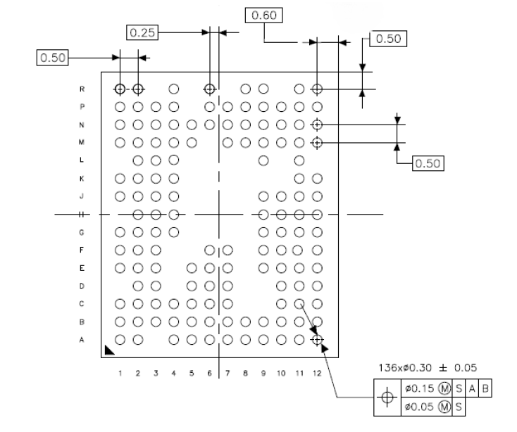
I've designed the footprint for the controller. Land dia is 0.24mm. My board is having six layers and i have used several vias for taking connection out of the controller. The vias i used were 0.15mm drill dia and 0.30mm regular pad. When i sent the gerber file to PCB fab house, they asked for some correction since their minimum IAR/OAR is 0.125mm. They found minimum OAR/IAR around 0.025mm for the drills of 0.15mm end dia. Their formula to calculate annular ring is as follows :
OAR / IAR = (Copper pad diameter - TOOLSIZE)/2
TOOLSIZE = ENDSIZE + 0.15mm for all PTH holes
+ 0.05mm for all NPTH holes
My question is how can i correct m design according to their requirement ? I have to choose copper pad dia of 0.55mm(for a drill of 0.15mm) to meet their standards. But since its a tight layout using .55mm vias will be practically impossible(pad to conductor spacing recommended by the fab house is 0.127mm). How can i complete my design from this challenges?
Any help would be appreciated.....