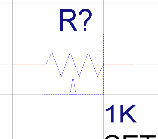
I'm sure I am missing a simple setting but after spending too much time looking for it I figured I'd come here. I want to have a smaller grid for component creation than for schematic creation, so I can create symbols in finer detail. For instance, below is a photo of the stock potentiometer, which clearly has lines that are not docked to the regular grid (1-1 pin spacing). However when I try to replicate it my lines snap to the grid. Any help would be appreciated.
↧
