Hi All:
How do we allow uncoupled diffpairs in a bga region, but do not allow anywhere else ?
Thanks,
Les
Hi All:
How do we allow uncoupled diffpairs in a bga region, but do not allow anywhere else ?
Thanks,
Les
Hi, I have Orcad Capture v16.6 and I am trying to set up the Tcl/TK utility PDF Export to use PDFCreator.exe as its PS to PDF converter. The problem I have is that the PDFCreator print list appears and runs for a few seconds and then locks up. It creates a pdf file but that file is broken and Adobe Acrobat cannot read it or fix it (not a complete file probably).
I have checked the postscript output (CapOutput.ps) by using an online converter and I get a good pdf from that although I can't get the CapPropMark.ps to create a properties pdf. I don't want to stay with the online solution because I run into file size problems with a full size design (CapOutput.ps = 86Mb, CapPropMark.ps = 320Mb).
Does anybody else use PDFCreator for this job and is there a particular setup needed? At present I select "Ghostscript / equivalent" for the converter and substitute the path to PDFCreator as follows
{C:\Program Files (x86)\PDFCreator\PDFCreator.exe} -sDEVICE=pdfwrite -sOutputFile=$::capPdfUtil::mPdfFilePath -dBATCH -dNOPAUSE $::capPdfUtil::mPSFilePath
Perhaps there are some changes I should make to this line? I might add that PDFCreator works fine as a normal print to pdf convertor.
Thanks in advance,
Jim O'Mahony
Hi
Sometimes I need to move the whole circuit or portion of a layout from top to bottom or via versa.
This is a permanent move, not just pressing on the Flip button.
I just wonder if anyone has a good way to do this and retaining all connections, parts and vias locations.
Dave, if you read this, please help.
Thanks
Regards,
TiBo
Hi All
Is there any way by which we can make a button and assign it a script in allegro PCB EDITOR.
Thanks
NWK
Hi All
Is there any way by which we can automatically route a portion of PCB (for e.g a circuit) and return to the main pcb?
Regards
NWK
Hi all,
This is probably very simple, but I can't find the answer anywhere.
I've created a few symbols in OrCAD, and their associated footprints in Allegro to use in designs. I'd like to assign manufacturer / manufacturer PN / vendor / vendor PN to the part itself, so whenever I use it in any design it is automatically part of the bill of material. Right now, I have to add the info in every time.
Again, I'm sure this is very simple but I am having no luck. Any help is appreciated.
I just upgraded my win 7 to win 10. Both OrCad PCB Editor and OrCad capture are running extremely slow. It take about 2 minutes for the software to come up, and then every command take at 30 seconds. I have looked at task manager, the CPU usage goes up to about 99% and stays that high even after I close OrCad. Any I dea why this is happening before I go back to win 7? Appreciate your help.
Hello,
I've been doing some research on this but can't find anything in the forums. I'm trying to output a BOM with all like parts on 1 line, to condense the list and make purchasing easier.
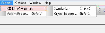
I start the BOM by going to Reports -> CIS Bill of Materials -> Standard. (photo 1)
For simplicity, my output format is only Part Reference, Quantity, Value. (photo 2) I have the Part Reference Options set as Standard.

However when I output the file, it is still giving each Part Reference its own line, as shown in photo 3. I'm not sure why this is happening. Any ideas?

I am wondering if it is necessary to specify a soldermask opening in the padstack for a padless nonplated hole, such as might be used for connector housing locating bosses or split barbs, snap-in plastic standoffs, etc. or if a padstack can just have the drilled hole and smaller diameter drilled-away pad and leave the soldermask layer null.
Thanks,
Allan
Hi everyone,
I would like to add a hand tool that slides the design as the cursor moves, just like it is in Cadence Design Entry HDL schematic. Actually when middle mouse button is pressed, the action is similar to what I want. But I want an invert mouse action and also middle mouse button is not very usefull when you are using left mouse button at the same time. Right mouse button or space button would be useful for this kind of roaming mode.
I modified PCB designer in many ways. I added lots of scripts, shortcuts including skill functions that zooms in and out just like Orcad Layout 16.0.
Skill Reference does not include mouse and keyboard input action control only cursor get and warp actions. On the other hand "funckey" method is for pressed and released input.
Is there a method for input button is pressed but not released.
Thanks for the replies,
Hi
I have this circuit that I want to simulate in Pspice. I have been able to make the schematic so far as per the given circuit. The AD8336, AD736 and AD8551 have been added externally as they were not available in the Pspice library. I had downloaded the model files for these from the Analog Devices website and have added them looking up some tutorials and basically with the help of the net, as I'm a a complete newbie to Pspice or any analog circuit simulation software for that matter.
So, the current status is that I get some errors when I try to run the simulation. I'll try to explain the error a bit.
The .cir file for AD8336 contains the design parameters for AD8336 and also its sub circuits. I have added the libraray file for AD8336 and all the other externally added components to my design. But even then I have these errors coming up, saying the subcircuits used by AD8336 are undefined.
How do I rectify these?
Please help. I'm not able to comprehend the errors due to the fact that I'm not at all acquainted with this environment.
I'm including the .cir file for AD8336 as included in the schematic as there is no provision for attaching the file directly. Also included are the errors as shown in the systems log when I try running my simulation. Please help. Thanks a lot for all the help rendered.
P.S: X_U1 refers to AD8336
X_U2 refers to AD736
------------------------------------------------------------------------------------------*AD8336.cir*------------------------------------------------------------------------------------
.SUBCKT AD8336 GNEG GPOS INPN INPP PRAO PWRA VCOM VGAI VNEG VOUT VPOS
E_U4_E8 VPBUF 0 TABLE { V(VPOS, 0) }
+ ( (0,0)(2.8,0)(3.0,1.6)(5,3.6)(12,10.6)(15,13.6))uselim
E_U4_E9 VNBUF 0 TABLE { V(VNEG, 0) }
+ ( (-15,-13.6)(-12,-10.6)(-5,-3.6)(-3.0,-1.6)(-2.8,0)(0,0))uselim
X_U4_D5 PRAO VPBUF DC_1mV_1A_1V_1nA
C_U4_C3 0 U4_S3 1n
R_U4_R4 0 INPP 450K
C_U4_C5 0 U4_N24227 2.5p
E_U4_E7 U4_N254725 0 VALUE {V(U4_N349891,0)*V(POK,0)}
R_U4_R6 0 INPN 450k
X_U4_D15 VNBUF U4_S3 GEN_DIODE
C_U4_C1 INPN PRAO 2p
X_U4_D13 U4_S3 VPBUF GEN_DIODE
G_U4_G4 0 U4_N24227 U4_S3 0 1
C_U4_C4 INPN 0 6p
X_U4_D6 VNBUF PRAO DC_1mV_1A_1V_1nA
X_U4_S1 PWRAL 0 U4_N254725 U4_S3 PrA_U4_S1
E_U4_E6 U4_N349891 0 INPP INPN 1.0
C_U4_C2 INPP 0 6p
G_U4_G3 U4_N24227 PRAO TABLE { V(U4_N24227, PRAO) }
+ ( (-15,-60m)(-1m,-50m)(0,0)(1m,50m)(15,60m) )uselim
G_U2_G8 VNEG 0 PWRAL 0 11m
X_U2_U12 VNEG U2_N958367 COMPARATOR2 PARAMS: TH=-2.8
R_U2_R14 0 VNEG 50K
R_U2_R11 0 VPOS 50K
G_U2_G6 VNEG 0 POK 0 14m
X_U2_U16 U2_N968984 POK PWRAL AND
X_U2_U14 U2_N958933 U2_N958855 POK AND
R_U2_R13 0 VNEG 50K
V_U2_V1 U2_AGAINDB1 U2_AGAINDB2 12.04
G_U2_G3 0 U2_AGAINDB1 TABLE { V(VGN, VCOM) }
+ (
+ (-1.0,-14.0)(-0.7,-14.0)(-0.6,-12.5)(-0.52,-9.3)(0.0,17.0)(0.2,27.0)(0.4,37.0)(0.5,42.0)(0.6,46.0)(1.0,46.0)
+ )uselim
X_U2_D13 GPOS VPOS GEN_DIODE
R_U2_R8 0 U2_AGAINDB1 1
E_U2_E1 VGN 0 GPOS GNEG 1
X_U2_U15 U2_N967091 PWRA U2_N968984 COMPARATOR
G_U2_G7 VPOS 0 PWRAL 0 11m
X_U2_U13 U2_N958367 U2_N958855 INVERTER
E_U2_ABM1 AGAIN 0 VALUE { (10**(V(U2_AGAINDB2)/20))*V(POK) }
R_U2_R12 0 VPOS 50K
C_U2_C5 0 U2_AGAINDB1 20n
X_U2_U11 VPOS U2_N958933 COMPARATOR2 PARAMS: TH=2.8
G_U2_G5 VPOS 0 POK 0 14m
X_U2_D14 VNEG GNEG GEN_DIODE
E_U2_E2 U2_N967091 0 TABLE { V(VPOS, 0) }
+ ( (0,0)(3,0.7) (5,1.2)(12,3.2) )uselim
X_U2_D16 GNEG VPOS GEN_DIODE
X_U2_D15 VNEG GPOS GEN_DIODE
E_U3_E8 U3_CMOUT U3_N55982 VCOM 0 1
E_U3_ABM1 U3_N62113 0 VALUE { MIN(PWR(V(AGAIN),1),1.6) }
E_U3_E7 U3_N55982 0 TABLE { V(VGN, 0) }
+ (
+ (-0.7,-2m)(-0.6,-4m)(-0.5,-8m)(-0.45,-10m)(-0.4,-14m)(-0.35,-15m)(-0.3,-11m)(-0.25,-9m)(-0.2,-11m)(-0.1,-22m)(0.0,-25m)(0.1,-16m)
+ (0.2,-19m)(0.3,-32m)(0.4,-52m)(0.5,-80m)(0.6,-120m)(0.65,-128m)(0.7,-127m) )uselim
E_U3_ABM2 U3_N61993 0 VALUE { (V(U3_RIN)-V(U3_ROUT))/nonzero(V(U3_N62113)) }
G_U3_G3 U3_N48981 U3_N48971 TABLE { V(U3_N48981, U3_N48971) }
+ ( (-15,-75m)(-1m,-64.8m)(0,0)(1m,64.8m)(15,75m) )uselim
X_U3_D16 U3_N48949 VPBUF GEN_DIODE
C_U3_C4 U3_N249674 0 1n
E_U3_E3 U3_N249442 0 U3_N48949 0 1
G_U3_G5 U3_RIN U3_ROUT U3_N61993 0 1
E_U3_E4 U3_RIN 0 VALUE {V(VGAI,0)*V(AGAIN,0)}np
X_U3_D7 VNBUF VOUT DC_1mV_1A_1V_1nA
E_U3_E2 U3_N48981 U3_CMOUT U3_N249674 0 1
R_U3_R15 U3_N249442 U3_N249674 0.1
X_U3_D18 VNBUF VGAI GEN_DIODE
X_U3_D6 VOUT VPBUF DC_1mV_1A_1V_1nA
X_U3_D17 VGAI VPBUF GEN_DIODE
X_U3_S1 PWRAL 0 U3_ROUT U3_N48949 VGA_U3_S1
R_U3_R14 U3_N48971 VOUT 2.5
X_U3_D15 VNBUF U3_N48949 GEN_DIODE
C_U3_C3 0 U3_N48949 1n
.ENDS
.subckt PrA_U4_S1 1 2 3 4
S_U4_S1 3 4 1 2 _U4_S1
RS_U4_S1 1 2 1G
.MODEL _U4_S1 VSWITCH Roff=200 Ron=100 Voff=0.25V Von=0.75V
.ends PrA_U4_S1
.subckt VGA_U3_S1 1 2 3 4
S_U3_S1 3 4 1 2 _U3_S1
RS_U3_S1 1 2 1G
.MODEL _U3_S1 VSWITCH Roff=10 Ron=.001 Voff=0.25V Von=0.75V
.ends VGA_U3_S1
.subckt GEN_DIODE 1 2
D1 1 2 DI2D
.model DI2D D Is=1e-14 Cjo=.1pF Rs=.1
.ends GEN_DIODE
.subckt DC_1mV_1A_1V_1nA A C
G1 A C TABLE { V(A, C) } ( (-1,-1n)(0,0)(1m,1) (2m,10) (3m,1000) )
.ends DC_1mV_1A_1V_1nA
.SUBCKT COMPARATOR2 INP OUT
+ PARAMs: TH=1
EOUT OUT 0 VALUE { IF( V(INP)>TH,1,0) }
.ends COMPARATOR2
.SUBCKT AND A B OUT
EOUT OUT 0 VALUE { IF( V(A)>0.5 & V(B)>0.5,1,0) }
.ends AND
.SUBCKT INVERTER IN OUT
EOUT OUT 0 VALUE { IF( V(IN)<0.5,1,0) }
.ends INVERTER
.SUBCKT COMPARATOR INP INM OUT
EOUT OUT 0 VALUE { IF( V(INP)>V(INM),1,0) }
.ends COMPARATOR
WARNING(ORPSIM-15188): There are no devices in this circuit
----------------------------------------------------------------------------- *Errors as in the system log*-----------------------------------------------------------------------
****** PSpice Lite (October 2012) ****** ID# 10813 ****
** Profile: "SCHEMATIC1-AGC Analysis" [ C:\OrCAD\OrCAD_16.6_Lite\tools\capture\agc_sim-pspicefiles\schematic1\agc analysis.sim ]
**** CIRCUIT DESCRIPTION
******************************************************************************
** Creating circuit file "AGC Analysis.cir"
** WARNING: THIS AUTOMATICALLY GENERATED FILE MAY BE OVERWRITTEN BY SUBSEQUENT SIMULATIONS
*Libraries:
* Profile Libraries :
* Local Libraries :
.LIB "C:/OrCAD/OrCAD_16.6_Lite/tools/pspice/library/ad736.lib"
.LIB "C:/OrCAD/OrCAD_16.6_Lite/tools/pspice/library/ad8551.lib"
.LIB "C:/OrCAD/OrCAD_16.6_Lite/tools/pspice/library/ad8336.lib"
* From [PSPICE NETLIST] section of C:\Users\Sakshi_Project_staff\AppData\Roaming\SPB_16.6\cdssetup\OrCAD_PSpice/16.6.0/PSpice.ini fi
.lib "nomd.lib"
*Analysis directives:
.TRAN 0 10ms 0
.OPTIONS ADVCONV
.PROBE64 V(alias(*)) I(alias(*)) W(alias(*)) D(alias(*)) NOISE(alias(*))
.INC "..\SCHEMATIC1.net"
**** INCLUDING SCHEMATIC1.net ****
* source AGC_SIM
V_V5 N13626 GND 5Vdc
X_U1 N13234 N13194 N13510 GND N13478 GND GND N13478 N13910 N133221
+ N13784 AD8336
R_R4 GND N13194 1k TC=0,0
C_C9 GND N13330 4.7n TC=0,0
R_R6 N13258 N13290 10k TC=0,0
X_U2 GND N13590 N15826 N13578 GND N13626 N13290 N13310 AD736
V_V3 N13784 GND 5Vdc
V_V1 GND N13030 5Vdc
R_R7 N133221 N13330 100 TC=0,0
C_C3 GND N13082 0.1u TC=0,0
C_C5 N13234 N13258 0.022u TC=0,0
V_V6 GND N13578 -5Vdc
R_R5 N13230 N13258 10k TC=0,0
C_C11 N13510 N13478 1n TC=0,0
C_C1 GND N13030 0.1u TC=0,0
R_R10 N13510 N13478 1k TC=0,0
C_C6 N13578 N13310 33u TC=0,0
V_V4 GND N13672 5Vdc
R_R1 N13118 N13082 9.09k TC=0,0
R_R9 N13768 N13510 1k TC=0,0
X_U3 N13672 N13234 GND N13258 N13648 AD8551
R_R3 N13194 N13082 1k TC=0,0
C_C4 N13230 N13234 2.2u TC=0,0
R_R11 GND N13590 1Meg TC=0,0
C_C7 N13330 OUTPUT 10u TC=0,0
C_C10 N13590 OUTPUT 0.1u TC=0,0
R_R13 N13118 N13648 500 TC=0,0
V_V2 N13910 GND -5Vdc
R_R12 GND N13648 500 TC=0,0
C_C12 N15826 N13290 10u TC=0,0
V_V9 N13768 GND AC 5V
+SIN 0V 5V 50 0 0 0
**** RESUMING "AGC Analysis.cir" ****
.END
INFO(ORPSIM-15423): Unable to find index file ad736.ind for library file ad736.lib.
INFO(ORPSIM-15422): Making new index file ad736.ind for library file ad736.lib.
Index has 1 entries from 1 file(s).
INFO(ORPSIM-15423): Unable to find index file ad8551.ind for library file ad8551.lib.
INFO(ORPSIM-15422): Making new index file ad8551.ind for library file ad8551.lib.
Index has 1 entries from 1 file(s).
**** EXPANSION OF SUBCIRCUIT X_U1 ****
X_U1.E_U4_E8 X_U1.VPBUF 0 TABLE { V(10#, 0) } 0 0 2.8 0 3.0 1.6 5 3.6
+ 12 10.6 15 13.6 uselim
------------------$
ERROR(ORPSIM-16152): Invalid number
$
ERROR(ORPSIM-16049): Values must be monotonic increasing
+ E_U4_E9 VNBUF 0 TABLE { V(8#, 0) } -15 -13.6 -12 -10.6 -5 -3.6 -3.0
+ -1.6 -2.8 0 0 0 uselim
X_U1.X_U4_D5 N13478 X_U1.VPBUF DC_1mV_1A_1V_1nA
X_U1.C_U4_C3 0 X_U1.U4_S3 1n
X_U1.R_U4_R4 0 GND 450K
X_U1.C_U4_C5 0 X_U1.U4_N24227 2.5p
X_U1.E_U4_E7 X_U1.U4_N254725 0 VALUE {V(U4_N349891,0)*V(POK,0)}
X_U1.R_U4_R6 0 N13510 450k
X_U1.X_U4_D15 X_U1.VNBUF X_U1.U4_S3 GEN_DIODE
X_U1.C_U4_C1 N13510 N13478 2p
X_U1.X_U4_D13 X_U1.U4_S3 X_U1.VPBUF GEN_DIODE
X_U1.G_U4_G4 0 X_U1.U4_N24227 X_U1.U4_S3 0 1
X_U1.C_U4_C4 N13510 0 6p
X_U1.X_U4_D6 X_U1.VNBUF N13478 DC_1mV_1A_1V_1nA
X_U1.X_U4_S1 X_U1.PWRAL 0 X_U1.U4_N254725 X_U1.U4_S3 PrA_U4_S1
X_U1.E_U4_E6 X_U1.U4_N349891 0 GND N13510 1.0
X_U1.C_U4_C2 GND 0 6p
X_U1.G_U4_G3 X_U1.U4_N24227 N13478 TABLE { V(U4_N24227, 4#) } -15
+ -60m -1m -50m 0 0 1m 50m 15 60m uselim
----------------------------------$
ERROR(ORPSIM-16152): Invalid number
$
ERROR(ORPSIM-16049): Values must be monotonic increasing
+ G_U2_G8 8 0 PWRAL 0 11m
X_U1.X_U2_U12 PARAMS X_U2_U12.TH -2.8 N13910 X_U1.U2_N958367
+ COMPARATOR2
X_U1.R_U2_R14 0 N13910 50K
X_U1.R_U2_R11 0 N13784 50K
X_U1.G_U2_G6 N13910 0 X_U1.POK 0 14m
X_U1.X_U2_U16 X_U1.U2_N968984 X_U1.POK X_U1.PWRAL AND
X_U1.X_U2_U14 X_U1.U2_N958933 X_U1.U2_N958855 X_U1.POK AND
X_U1.R_U2_R13 0 N13910 50K
X_U1.V_U2_V1 X_U1.U2_AGAINDB1 X_U1.U2_AGAINDB2 12.04
X_U1.G_U2_G3 0 X_U1.U2_AGAINDB1 TABLE { V(VGN, 6#) } -1.0 -14.0 -0.7
+ -14.0 -0.6 -12.5 -0.52 -9.3 0.0 17.0 0.2 27.0 0.4 37.0 0.5 42.0 0.6
+ 46.0 1.0 46.0 uselim
----------------$
ERROR(ORPSIM-16152): Invalid number
$
ERROR(ORPSIM-16049): Values must be monotonic increasing
+ X_U2_D13 1 10 GEN_DIODE
X_U1.R_U2_R8 0 X_U1.U2_AGAINDB1 1
X_U1.E_U2_E1 X_U1.VGN 0 N13194 N13234 1
X_U1.X_U2_U15 X_U1.U2_N967091 GND X_U1.U2_N968984 COMPARATOR
X_U1.G_U2_G7 N13784 0 X_U1.PWRAL 0 11m
X_U1.X_U2_U13 X_U1.U2_N958367 X_U1.U2_N958855 INVERTER
X_U1.E_U2_ABM1 X_U1.AGAIN 0 VALUE { (10**(V(U2_AGAINDB2)/20))*V(POK)
+ }
X_U1.R_U2_R12 0 N13784 50K
X_U1.C_U2_C5 0 X_U1.U2_AGAINDB1 20n
X_U1.X_U2_U11 PARAMS X_U2_U11.TH 2.8 N13784 X_U1.U2_N958933
+ COMPARATOR2
X_U1.G_U2_G5 N13784 0 X_U1.POK 0 14m
X_U1.X_U2_D14 N13910 N13234 GEN_DIODE
X_U1.E_U2_E2 X_U1.U2_N967091 0 TABLE { V(10#, 0) } 0 0 3 0.7 5 1.2 12
+ 3.2 uselim
------$
ERROR(ORPSIM-16152): Invalid number
$
ERROR(ORPSIM-16049): Values must be monotonic increasing
+ X_U2_D16 0 10 GEN_DIODE
X_U1.X_U2_D15 N13910 N13194 GEN_DIODE
X_U1.E_U3_E8 X_U1.U3_CMOUT X_U1.U3_N55982 GND 0 1
X_U1.E_U3_ABM1 X_U1.U3_N62113 0 VALUE { MIN(PWR(V(AGAIN),1),1.6) }
X_U1.E_U3_E7 X_U1.U3_N55982 0 TABLE { V(VGN, 0) } -0.7 -2m -0.6 -4m
+ -0.5 -8m -0.45 -10m -0.4 -14m -0.35 -15m -0.3 -11m -0.25 -9m -0.2
+ -11m -0.1 -22m 0.0 -25m 0.1 -16m 0.2 -19m 0.3 -32m 0.4 -52m 0.5
+ -80m 0.6 -120m 0.65 -128m 0.7 -127m uselim
--------------------------------------$
ERROR(ORPSIM-16152): Invalid number
$
ERROR(ORPSIM-16049): Values must be monotonic increasing
+ E_U3_ABM2 U3_N61993 0 VALUE { (V(U3_RIN)-V(U3_ROUT))/nonzero(V(U3_N62113))
+ }
X_U1.G_U3_G3 X_U1.U3_N48981 X_U1.U3_N48971 TABLE { V(U3_N48981, U3_N48971)
+ } -15 -75m -1m -64.8m 0 0 1m 64.8m 15 75m uselim
--------------------------------------------$
ERROR(ORPSIM-16152): Invalid number
$
ERROR(ORPSIM-16049): Values must be monotonic increasing
ERROR(ORPSIM-15108): Subcircuit DC_1mV_1A_1V_1nA used by X_U1.X_U4_D5 is undefined
ERROR(ORPSIM-15108): Subcircuit GEN_DIODE used by X_U1.X_U4_D15 is undefined
ERROR(ORPSIM-15108): Subcircuit GEN_DIODE used by X_U1.X_U4_D13 is undefined
ERROR(ORPSIM-15108): Subcircuit DC_1mV_1A_1V_1nA used by X_U1.X_U4_D6 is undefined
ERROR(ORPSIM-15108): Subcircuit PrA_U4_S1 used by X_U1.X_U4_S1 is undefined
ERROR(ORPSIM-15108): Subcircuit COMPARATOR2 used by X_U1.X_U2_U12 is undefined
ERROR(ORPSIM-15108): Subcircuit AND used by X_U1.X_U2_U16 is undefined
ERROR(ORPSIM-15108): Subcircuit AND used by X_U1.X_U2_U14 is undefined
ERROR(ORPSIM-15108): Subcircuit COMPARATOR used by X_U1.X_U2_U15 is undefined
ERROR(ORPSIM-15108): Subcircuit INVERTER used by X_U1.X_U2_U13 is undefined
ERROR(ORPSIM-15108): Subcircuit COMPARATOR2 used by X_U1.X_U2_U11 is undefined
ERROR(ORPSIM-15108): Subcircuit GEN_DIODE used by X_U1.X_U2_D14 is undefined
ERROR(ORPSIM-15108): Subcircuit GEN_DIODE used by X_U1.X_U2_D15 is undefined
ERROR(ORPSIM-15108): Subcircuit DC_1mV_1A_1V_1nA used by X_U1.X_U3_D7 is undefined
ERROR(ORPSIM-15108): Subcircuit GEN_DIODE used by X_U1.X_U3_D18 is undefined
ERROR(ORPSIM-15108): Subcircuit DC_1mV_1A_1V_1nA used by X_U1.X_U3_D6 is undefined
ERROR(ORPSIM-15108): Subcircuit GEN_DIODE used by X_U1.X_U3_D17 is undefined
ERROR(ORPSIM-15108): Subcircuit VGA_U3_S1 used by X_U1.X_U3_S1 is undefined
ERROR(ORPSIM-15108): Subcircuit GEN_DIODE used by X_U1.X_U3_D15 is undefined
ERROR(ORPSIM-15108): Subcircuit AEIOPAMP0 used by X_U2.X3 is undefined
ERROR(ORPSIM-15108): Subcircuit AEIOPAMP1 used by X_U2.X1 is undefined
Hi i have downloaded latest file RotateSilkAssyRD.il. it is V2.2.
Now when i tried to load the file, i use this along with nsware code:
Data of "allegro.ilinit"
; load the nsWare framework and products
load("./RotateSilkAssyRD.il")
load("./nsWare/nsware.il" "nsware" )
it loads only nsware in toolbar. how do i use the silkscreen script? please elaborate.
thanks.
Hi all,
I'm setting a region in the BGA area for 4 mils spacing line/line. My 90 ohm pair came out to be 3.7mil spacing so it violates this rule. I know I can lower the constraints with in the region to meet this demand, but I prefer to keep the spec at 4 mils for rest of the traces.
I have checked the setting in Setup>constraints>modes>electrical options>Differential Pair Constraints which helps me maintain the line/space, but it still shows the DRC for line/line spacing for violating the 4 mil space.
Is there a way to avoid this DRC within this region without editing the region shape or adding another region?
Also my default constraints are set to 5 mil spacing it does not DRC the diffpair gap. it's only for the region area.
Please let me know if anyone has suggestions.
I have this circuit to be simulated in Pspice. I'm a complete newbie to it. But so far have managed to make the schematic (adding external components, which were not available already in the library).
[![enter image description here][1]][1]
I have added models for AD8336, AD736 and AD8551 externally (models for which were available on Analaog devices website). Now when I try to run my simulation, I get errors as to the sub circuits used by AD8336 and AD736 are undefined (although I have added the libraries for these components to my design in the simulation profile).
[![enter image description here][2]][2]
P.S: I have included the links for the .cir file (model file) for AD8336 and AD736 here in for your reference as well as the list of errors that I get in my system log on running the simulation. Please help me resolve this
Thanks!
Error log on simulation :
**** 10/07/15 10:45:53 ****** PSpice Lite (October 2012) ****** ID# 10813 ****
** Profile: "SCHEMATIC1-AGC Analysis" [ C:\OrCAD\OrCAD_16.6_Lite\tools\capture\agc_sim-pspicefiles\schematic1\agc analysis.sim ]
**** CIRCUIT DESCRIPTION
******************************************************************************
** Creating circuit file "AGC Analysis.cir"
** WARNING: THIS AUTOMATICALLY GENERATED FILE MAY BE OVERWRITTEN BY SUBSEQUENT SIMULATIONS
*Libraries:
* Profile Libraries :
* Local Libraries :
.LIB "C:/OrCAD/OrCAD_16.6_Lite/tools/pspice/library/ad736.lib"
.LIB "C:/OrCAD/OrCAD_16.6_Lite/tools/pspice/library/ad8551.lib"
.LIB "C:/OrCAD/OrCAD_16.6_Lite/tools/pspice/library/ad8336.lib"
* From [PSPICE NETLIST] section of C:\Users\Sakshi_Project_staff\AppData\Roaming\SPB_16.6\cdssetup\OrCAD_PSpice/16.6.0/PSpice.ini fi
.lib "nomd.lib"
*Analysis directives:
.TRAN 0 10ms 0
.OPTIONS ADVCONV
.PROBE64 V(alias(*)) I(alias(*)) W(alias(*)) D(alias(*)) NOISE(alias(*))
.INC "..\SCHEMATIC1.net"
**** INCLUDING SCHEMATIC1.net ****
* source AGC_SIM
V_V5 N13626 GND 5Vdc
X_U1 N13234 N13194 N13510 GND N13478 GND GND N13478 N13910 N133221
+ N13784 AD8336
R_R4 GND N13194 1k TC=0,0
C_C9 GND N13330 4.7n TC=0,0
R_R6 N13258 N13290 10k TC=0,0
X_U2 GND N13590 N15826 N13578 GND N13626 N13290 N13310 AD736
V_V3 N13784 GND 5Vdc
V_V1 GND N13030 5Vdc
R_R7 N133221 N13330 100 TC=0,0
C_C3 GND N13082 0.1u TC=0,0
C_C5 N13234 N13258 0.022u TC=0,0
V_V6 GND N13578 -5Vdc
R_R5 N13230 N13258 10k TC=0,0
C_C11 N13510 N13478 1n TC=0,0
C_C1 GND N13030 0.1u TC=0,0
R_R10 N13510 N13478 1k TC=0,0
C_C6 N13578 N13310 33u TC=0,0
V_V4 GND N13672 5Vdc
R_R1 N13118 N13082 9.09k TC=0,0
R_R9 N13768 N13510 1k TC=0,0
X_U3 N13672 N13234 GND N13258 N13648 AD8551
R_R3 N13194 N13082 1k TC=0,0
C_C4 N13230 N13234 2.2u TC=0,0
R_R11 GND N13590 1Meg TC=0,0
C_C7 N13330 OUTPUT 10u TC=0,0
C_C10 N13590 OUTPUT 0.1u TC=0,0
R_R13 N13118 N13648 500 TC=0,0
V_V2 N13910 GND -5Vdc
R_R12 GND N13648 500 TC=0,0
C_C12 N15826 N13290 10u TC=0,0
V_V9 N13768 GND AC 5V
+SIN 0V 5V 50 0 0 0
**** RESUMING "AGC Analysis.cir" ****
.END
**** EXPANSION OF SUBCIRCUIT X_U1 ****
X_U1.E_U4_E8 X_U1.VPBUF 0 TABLE { V(10#, 0) } 0 0 2.8 0 3.0 1.6 5 3.6
+ 12 10.6 15 13.6 uselim
------------------$
ERROR(ORPSIM-16152): Invalid number
$
ERROR(ORPSIM-16049): Values must be monotonic increasing
+ E_U4_E9 VNBUF 0 TABLE { V(8#, 0) } -15 -13.6 -12 -10.6 -5 -3.6 -3.0
+ -1.6 -2.8 0 0 0 uselim
X_U1.X_U4_D5 N13478 X_U1.VPBUF DC_1mV_1A_1V_1nA
X_U1.C_U4_C3 0 X_U1.U4_S3 1n
X_U1.R_U4_R4 0 GND 450K
X_U1.C_U4_C5 0 X_U1.U4_N24227 2.5p
X_U1.E_U4_E7 X_U1.U4_N254725 0 VALUE {V(U4_N349891,0)*V(POK,0)}
X_U1.R_U4_R6 0 N13510 450k
X_U1.X_U4_D15 X_U1.VNBUF X_U1.U4_S3 GEN_DIODE
X_U1.C_U4_C1 N13510 N13478 2p
X_U1.X_U4_D13 X_U1.U4_S3 X_U1.VPBUF GEN_DIODE
X_U1.G_U4_G4 0 X_U1.U4_N24227 X_U1.U4_S3 0 1
X_U1.C_U4_C4 N13510 0 6p
X_U1.X_U4_D6 X_U1.VNBUF N13478 DC_1mV_1A_1V_1nA
X_U1.X_U4_S1 X_U1.PWRAL 0 X_U1.U4_N254725 X_U1.U4_S3 PrA_U4_S1
X_U1.E_U4_E6 X_U1.U4_N349891 0 GND N13510 1.0
X_U1.C_U4_C2 GND 0 6p
X_U1.G_U4_G3 X_U1.U4_N24227 N13478 TABLE { V(U4_N24227, 4#) } -15
+ -60m -1m -50m 0 0 1m 50m 15 60m uselim
----------------------------------$
ERROR(ORPSIM-16152): Invalid number
$
ERROR(ORPSIM-16049): Values must be monotonic increasing
+ G_U2_G8 8 0 PWRAL 0 11m
X_U1.X_U2_U12 PARAMS X_U2_U12.TH -2.8 N13910 X_U1.U2_N958367
+ COMPARATOR2
X_U1.R_U2_R14 0 N13910 50K
X_U1.R_U2_R11 0 N13784 50K
X_U1.G_U2_G6 N13910 0 X_U1.POK 0 14m
X_U1.X_U2_U16 X_U1.U2_N968984 X_U1.POK X_U1.PWRAL AND
X_U1.X_U2_U14 X_U1.U2_N958933 X_U1.U2_N958855 X_U1.POK AND
X_U1.R_U2_R13 0 N13910 50K
X_U1.V_U2_V1 X_U1.U2_AGAINDB1 X_U1.U2_AGAINDB2 12.04
X_U1.G_U2_G3 0 X_U1.U2_AGAINDB1 TABLE { V(VGN, 6#) } -1.0 -14.0 -0.7
+ -14.0 -0.6 -12.5 -0.52 -9.3 0.0 17.0 0.2 27.0 0.4 37.0 0.5 42.0 0.6
+ 46.0 1.0 46.0 uselim
----------------$
ERROR(ORPSIM-16152): Invalid number
$
ERROR(ORPSIM-16049): Values must be monotonic increasing
+ X_U2_D13 1 10 GEN_DIODE
X_U1.R_U2_R8 0 X_U1.U2_AGAINDB1 1
X_U1.E_U2_E1 X_U1.VGN 0 N13194 N13234 1
X_U1.X_U2_U15 X_U1.U2_N967091 GND X_U1.U2_N968984 COMPARATOR
X_U1.G_U2_G7 N13784 0 X_U1.PWRAL 0 11m
X_U1.X_U2_U13 X_U1.U2_N958367 X_U1.U2_N958855 INVERTER
X_U1.E_U2_ABM1 X_U1.AGAIN 0 VALUE { (10**(V(U2_AGAINDB2)/20))*V(POK)
+ }
X_U1.R_U2_R12 0 N13784 50K
X_U1.C_U2_C5 0 X_U1.U2_AGAINDB1 20n
X_U1.X_U2_U11 PARAMS X_U2_U11.TH 2.8 N13784 X_U1.U2_N958933
+ COMPARATOR2
X_U1.G_U2_G5 N13784 0 X_U1.POK 0 14m
X_U1.X_U2_D14 N13910 N13234 GEN_DIODE
X_U1.E_U2_E2 X_U1.U2_N967091 0 TABLE { V(10#, 0) } 0 0 3 0.7 5 1.2 12
+ 3.2 uselim
------$
ERROR(ORPSIM-16152): Invalid number
$
ERROR(ORPSIM-16049): Values must be monotonic increasing
+ X_U2_D16 0 10 GEN_DIODE
X_U1.X_U2_D15 N13910 N13194 GEN_DIODE
X_U1.E_U3_E8 X_U1.U3_CMOUT X_U1.U3_N55982 GND 0 1
X_U1.E_U3_ABM1 X_U1.U3_N62113 0 VALUE { MIN(PWR(V(AGAIN),1),1.6) }
X_U1.E_U3_E7 X_U1.U3_N55982 0 TABLE { V(VGN, 0) } -0.7 -2m -0.6 -4m
+ -0.5 -8m -0.45 -10m -0.4 -14m -0.35 -15m -0.3 -11m -0.25 -9m -0.2
+ -11m -0.1 -22m 0.0 -25m 0.1 -16m 0.2 -19m 0.3 -32m 0.4 -52m 0.5
+ -80m 0.6 -120m 0.65 -128m 0.7 -127m uselim
--------------------------------------$
ERROR(ORPSIM-16152): Invalid number
$
ERROR(ORPSIM-16049): Values must be monotonic increasing
+ E_U3_ABM2 U3_N61993 0 VALUE { (V(U3_RIN)-V(U3_ROUT))/nonzero(V(U3_N62113))
+ }
X_U1.G_U3_G3 X_U1.U3_N48981 X_U1.U3_N48971 TABLE { V(U3_N48981, U3_N48971)
+ } -15 -75m -1m -64.8m 0 0 1m 64.8m 15 75m uselim
--------------------------------------------$
ERROR(ORPSIM-16152): Invalid number
$
ERROR(ORPSIM-16049): Values must be monotonic increasing
ERROR(ORPSIM-15108): Subcircuit DC_1mV_1A_1V_1nA used by X_U1.X_U4_D5 is undefined
ERROR(ORPSIM-15108): Subcircuit GEN_DIODE used by X_U1.X_U4_D15 is undefined
ERROR(ORPSIM-15108): Subcircuit GEN_DIODE used by X_U1.X_U4_D13 is undefined
ERROR(ORPSIM-15108): Subcircuit DC_1mV_1A_1V_1nA used by X_U1.X_U4_D6 is undefined
ERROR(ORPSIM-15108): Subcircuit PrA_U4_S1 used by X_U1.X_U4_S1 is undefined
ERROR(ORPSIM-15108): Subcircuit COMPARATOR2 used by X_U1.X_U2_U12 is undefined
ERROR(ORPSIM-15108): Subcircuit AND used by X_U1.X_U2_U16 is undefined
ERROR(ORPSIM-15108): Subcircuit AND used by X_U1.X_U2_U14 is undefined
ERROR(ORPSIM-15108): Subcircuit COMPARATOR used by X_U1.X_U2_U15 is undefined
ERROR(ORPSIM-15108): Subcircuit INVERTER used by X_U1.X_U2_U13 is undefined
ERROR(ORPSIM-15108): Subcircuit COMPARATOR2 used by X_U1.X_U2_U11 is undefined
ERROR(ORPSIM-15108): Subcircuit GEN_DIODE used by X_U1.X_U2_D14 is undefined
ERROR(ORPSIM-15108): Subcircuit GEN_DIODE used by X_U1.X_U2_D15 is undefined
ERROR(ORPSIM-15108): Subcircuit DC_1mV_1A_1V_1nA used by X_U1.X_U3_D7 is undefined
ERROR(ORPSIM-15108): Subcircuit GEN_DIODE used by X_U1.X_U3_D18 is undefined
ERROR(ORPSIM-15108): Subcircuit DC_1mV_1A_1V_1nA used by X_U1.X_U3_D6 is undefined
ERROR(ORPSIM-15108): Subcircuit GEN_DIODE used by X_U1.X_U3_D17 is undefined
ERROR(ORPSIM-15108): Subcircuit VGA_U3_S1 used by X_U1.X_U3_S1 is undefined
ERROR(ORPSIM-15108): Subcircuit GEN_DIODE used by X_U1.X_U3_D15 is undefined
ERROR(ORPSIM-15108): Subcircuit AEIOPAMP0 used by X_U2.X3 is undefined
ERROR(ORPSIM-15108): Subcircuit AEIOPAMP1 used by X_U2.X1 is undefined
Edit: The links to the the ad8336.cir model file and the AD736.cir model file are as follows in the same order:
http://textuploader.com/ankv9! (AD8336.cir)
http://textuploader.com/ankvp! (AD736.cir)
[1]: http://i.stack.imgur.com/Ro1gr.jpg
[2]: http://i.stack.imgur.com/GrqRL.jpg
Does anyone else draw boxes around sub-circuits on flat designs? It seems like there should be some sort of "Box Tool" to help divide your schematic up. We typically end up using wires, drawing wires around circuits and changing the color and/or wire pattern. The problem with that is then there's a possibility of you accidentally "connecting" to your box, and then you short signals out. If anyone has any other ideas or thoughts on how to do this, I would appreciate hearing a solution.
Usually my key 'r' that I assigned to rotate components works perfectly, 360 degrees.On selected designs it just does a quarter turn, and I have to go back the regular rotate in right click.
Any suggestions as to why this might be?
My part manager is missing in CIS. I've gone to View - Toolbar - and selected Part Manger on and off and on. This didn't help. Please help!!
Thanks,
Jill
When I was using Cadence Capture about 8 years ago at another company, we had the ability to add tables of parts to a design to allow us to add parts that were part of the BOM for design tracking purposes but not part of the schematic (e.g., documents). We could also (IIRC) overload properties on parts in the schematic when the correct part was not available in the parts database.
Flash forward to now, trying to do the same with OrCAD Design Entry CIS 16.6, and I am struggling with finding the correct approach for this. Has anyone else tried to do this and succeeded?
Thanks!
Hi all,
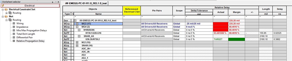
In one of our board, for a SRAM group which having series resistor's as terminators, for delay tuning, I wanted to add the traces from FPGA to resistor and from resistor to SRAM in a group to match its total length. But I'm unable to add the traces of before and after resistor in same group. Attached a screenshot as an example, in which MG4 is a match group and N19926395 is trace from FPGA to R and SRAM_A5 is trace from R to SRAM IC. I wanted to add both nets in same group which showing total length. How can I do it and for the whole group(A0 to A16)? Any other way? Any input will be appreciated.
Tool using: OrCAD PCB Designer Professional v16.6 with hotfix s055
Thank you,
Shiva.
Hi,
I have a RevA board file and its associated symbols and padstack located in a directory. Now for RevB I'm making few changes to some padstack and related symbols. For RevB, I created another directory which has all these new padstack and all symbols.
Now when I go yo Place-> Update Symbol, it doesnt fetch the new definition for the symbols and padstack from new directory. I also updated the PSMPATH and PADPATH variables. I checked it many times.
Is there a way around?