Quantcast
Channel: Cadence PCB Design Forum
Viewing all 5525 articles
Browse latest View live

CAPTURE: NETLIST_IGNORE for hierarchical objects?

$
0
0

Hello everyone

I cannot make this work, can you please help me undersatand if there is a way?
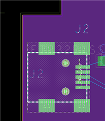
I'd like to ignore a hyerarchical object on a Schematic Page from routing on PCB Editor.

I have tried setting the NETLIST_IGNORE to TRUE for the hierarchical object, but DRC shows me that its elements are still being considered - the problem is there are situations where only one block instance should be excluded - besides that, selecting all the sub-components and setting the property is not as handy, obviously.

Is there a way?

If I go and set the NETLIST IGNORE for all the components in the block to true, they are being excluded as expected, of course.

Thanks


change footprint without orcad capture schematic

$
0
0

Hi all,

I need to change the footprint without orcad schematic.

for instance, there is a smd type usb footprint, I want to change this part to 5 pin header which mean same number of pins and nets

like this

regards.

Capture: how to reset annotation for selected parts

$
0
0

Hello everyone

Tried to reset refdefs for selected items with the annotation tool, but it looks like I'm unable to make it work (apparently).

This is an example:

After pressing OK, I'd expect J3 to be changed to J?, instead it stays the same. Console tells me "INFO(ORCAP-1379): Done updating part references"

What am I missing here?

If I try resetting the whole design, it works.

Thanks for your help and patience

PCB Editor: Component value class not showing on render

$
0
0

Hi there

I'm trying to show values on the silkscreen, using the Component value class. Problem is that apparently the values do not show up in the renderer (not sure how this affects Gerbers etc yet) unlike the RefDefs class.
See example below. The text of the Component Value>Silkscreen_top and RefDefs>Silkscreen_top have the same size and Photo width. One shows, unlike the other. Visibility set to Global On


Refdefs (Jx) show up, Compval (IN+ etc) does not.
What could be the setting to fix this?

Thanks

PCB Design Technical solution supports

$
0
0

Hi All

Here we published the link for All kind of PCB Design Technical solutions and Video tutorials 

https://rb.gy/frxudg\

Please watch and give your promotion and we expecting more supports from you peoples

Thanks

Route file difference between 17.2 and 17.4

$
0
0

For those of you that have slots in your board, we have found that there is a difference between the route file created from 17.2 and 17.4. Not sure why as the existing file from 17.2 always seemed to work. It looks like they are adding more information about the slot. 

17.2 route file

17.4 route

Picture of 17.2 slot dimensions. Begin and end drill holes

Picture of 17.4 slot dimensions. Begin and end plus top and bottom limits.

The only reason we found this was we are trying to use OSHPARK to build this board and the standard route file was not being accepted as valid. So we had to go into the file and delete some of the numbers in the file before OSHPARK would accept the file.

auto routing maximum layer

$
0
0

Hi all,

if I use OrCAD professional license and want to run auto-routing, what is maximum supporting layer?

As I know OrCAD Professional license support maximum 6 layer, and Allegro license support maximum 256.

am I right?

regard!

Bias Point: How show calculated value?

$
0
0

I Imagined there must be a way to do this. 

I'd like to show the Gate to Source voltage on a MOSFET instead of doing the calculation by hand. 
Is there a way to do that? I arrived to define a parameter based on the Bias point output file from Pspice, but I cannot understand how to show the calcluated value instead of the formula.

Is there a way/ alternative way to do that? In the following picture, I'd like to show a box with the 3.76V calculated value.

Of course I could chart using voltage differential probes, but I'd like to have something quick and easy to see as the bias point markers.


Bias Point: how to control rounding?

$
0
0

Hi there

Is there a way of rounding the values of the bias point to multiple of some values for instance or setting limits or setting the reference power for the unit (m, p, etc?)?

Just to remove clutter... in my DC simulation I'd like to reduce it by cutting off or rounding values - so that instead of having to read 846pA or 1.578e-30A to understand that no actual current is flowing,

I can have a simple 0A.Or in alternative require that all values for current are expressed, say, in mA wth the same rounding . Instead of having A here, mA there, nA elsewhere, pA, fA, uA .

I think you get what I mean ;)

Thanks!

So the question becomes: How rounding is controlled? I just found this: 

Advice needed: How manage Design alternatives

$
0
0

Hello everyone,

beginner here so I'm trying to undersand how best to best get organized to work with Capture.

I wonder what is the "best practice" to manage design alternatives (that is, different circuits functionally equivalent but potentially very different in terms of schematic.)


I'm currently using hierarchical blocks which I am plugging in and out of a "core" board for testing (currently replacing manually the block, till I find a smarter way to do this. Changing the implementation property of the hierarchical block  leads to some crashes of the app, still need to dig into that)

In the below "top level" schematic, every hierarchical block represent a physical different PCB. One of these blocks points to two hierachical block alternatives, here Board_interm_JFET and Board interm MOSFET.

I'm not completely happy as I'd like this to be better organized (I tried placing the alternatives as pages in the same Schematic, but that does not work when I try to convert into a PCB as all the components end up staged for the layout)

Is there a proper way to organize this? Please provide me some hints, I have looked at BOM Variants but if I undertstood properly is not the proper way.

Thanks!

PCB Editor: how show component properties on PCB

$
0
0

Hi there.

What is the working way to show the component Value on a PCB board ?

Tried adding in the Symbol drawing definition (dra) of the symbols a Label using the Layout>Display>Label>Value menu. Placed the placeholder, say , on Component_Value>Silkscreen_top

When I process the board, the values are properly transferred, as I can see routing the board.

Next I edit the text to match a size, whose Photo Witdth is not 0. Do the same for a text of say, the package_geometry class to test.
The Component_value class does not show up on the 3D view of the PCB, the PackageGeometry does.

So this looks like a dead end.

What am I doing wrong here?

Netlist Error

$
0
0

Hello

In schematic I enabled make swap to FPGA.

I got design with swapped lines in FPGA and I make back annotate.

And after it when I tried to run netlist, I got next error notification:

ERROR(SPCODD-409): Error at line 65 while loading the C:\Project\1579\Schematic\Temp\netlist\pstxnet.dat file. Unable to create the following new pin instance, IO_4A_AB16/DIFFIO_TX_B29P/DQ4B, as the pin definition was not found.

      Reference Designator: P1.

      Schematic Instance: @\ba1579-sd1-p1_01\.top_level(sch_1):bl2@\ba1579-sd1-p1_01\.fpga1_main(sch_1):bl42@\ba1579-sd1-p1_01\.fpga1_page5(sch_1):ins15430831@\ba1579-sd1-d19\.\5cgxfc4cu19_7b.normal\(chips) (MODULE: FPGA1_PAGE5; PART: 5CGXFC4CU19_7).

      Check the symbol and ensure that the pin definition is consistent.


ERROR(SPCODD-383): Error at line 65 in file C:\Project\1579\Schematic\Temp\netlist\pstxnet.dat. Unable to load the net list file. Run Packager-XL (Export - Physical) again.


Can you advise how can I resolve it?

Static Dummy net name auto assign respect to IC pin net name

$
0
0

Is there is any way to connect dummy net into IC pin NetNames. I know that there is option  in Assign net, but  I have 900+ Dummy net shape in my design.

I can't make it manual.

is there any way to do this into automation.

Thanks,

karthik.R

sigrity speedem simulator animation

$
0
0

I am playing with the speedem simulator in ESD mode and using a very simple circuit to simulate what happens in the case of an ESD discharge on one trace to close by traces.

I did that with a 4 layer board and i was able to get some nice 3 animations that were showing what is happening voltage wise over time.

This simple circuit i get no animation at all. the simple circuit is just 4 resistors on a two layer board. see attached images.

I did the same setup steps as with the 4 layer board.

the 2D graph shows what happens over time , but somehow it can not be animated in 3D , the play button is grayed out.

Please, how to create a peelable mask layer?

$
0
0

Hi.

I'm extremely new to Allegro, I've just bought 17.4 and over the course of the last 2 weeks have managed to generate a board,  produce the artwork and then create the Gerbers.

However the customer wants me to generate a peelable mask layer, essentially big circles of thick gunk covering the mounting holes so the solder doesn’t fill the holes when the board is placed in the solder wave machine.

I already know how to change the padstack for the mounting hole by using the padstack editor. Its obvious what to do for the drill, copper layers, solder screen and solder paste modifications.
I can see two other layers, there is a filmmask and coverlay. Prior they were set up as none so I thought I could utilise these for the peelable mask layer and so I added the necessary circles but try as I might I cannot see these additional layers at all even when global visibility is on and even if I add the layers as part of the cross section editor. That is Question 1, what are the filmmask and coverlay and why can’t I make them visible??

I know how to create additional layers of artwork by selecting the visibility of various attributes of the design and use 'add' in the Artwork Control Form' but I just can't manage to add a layer of a total of 4 circles, one for each mounting hole.

So question 2 is :- If for some reason the filmmask and coverlay are not the correct manner to generate the peelable mask layer how do I do it??

Many thanks. Andrew.


how to import the .mcm file on my board as an footprint? (importing .mcm or .sip file to .brd file)

$
0
0

Hi all,

I don't know well about between Allegro Package Designer and allegro PCB Designer file compatibility.

if someone create the bgm symbol with Allegro Package Designer, then the result file will be .mcm file or .sip file

as I know, To place the footprint, I have to have the .psm& .dra file (if I created by Allegro PCB Designer)

then if I want to place the package (footprint) with this .mcm file which I created by Allegro Package Designer on my board, How can I import the .mcm file on my board?

Is there any guide documentation about this?

best regard

17.20 (Electrically Connected) Mounting holes displayed in 3D as boxes or barrels - Reviving old thread...

$
0
0

Dear forum,

I am reviving this thread as I am seeing this problem when displaying a populated board in 3D. Since I design mounting holes as electrical components as I want to connect them to ie. GND, I have tried these options:

1. As a component with PLACE_BOUND_TOP (Or bottom) with property height = 0 mm

2. As a component with PLACE_BOUND_TOP (Or bottom) without any property added to the shapes.

2. As a component without the shapes above.

In neither of these cases, I get a 3D view representation of the board with the holes VISIBLE and NOT covered by black square boxes or barrels of some pre-defined height.

...

PCB Design YOUTUBE Channel for Practical Demo

$
0
0

Hi All

Here we published the link for All kind of PCB Design Technical solutions and Practical Demo 

https://cutt.ly/ykNZp5b

Please watch and Subscriber 

Thanks

120 pin header

$
0
0

Hi all,

Totally new to this, but been trying to get my head around it the last few days with a unrouted file I've been sent and thus been asked "route this!"

So I've come up against my first hurdle. It has a 120pin header which the manufacturers footprint appears to have exceptionally large pads. I would like to edit these ideally as one lump to make them smaller.

I know newbie questions are annoying, but here we go.. Where do I start?

Help with voltage source parameters

$
0
0

Hello,

I want to do AC analysis and transient analysis for an analog cicuit. I'm facing a problem for my source parameters. I can find two AC sources. In the menu "place"--> "PSpice component"-->"Source"-->"voltage sources".  There I have "AC" and "Sine"

Now, for the "Sine" source, I can set 4 parameters. 

       - VOFF for the offest i figured

       - FREQ for the frequency

       - VAMPL and AC. And I don't know what these are for and the difference between the two. 

The second source is "AC" and here i can parameter the "Vac" and "Vdc" which must be the DC votltage and AC voltage. I'm guessing that this source is for AC sweep simulations.

I'm using Cadence Allegro Entry CIS 17.2-2016

Thanx for your help!

Viewing all 5525 articles
Browse latest View live


Latest Images

<script src="https://jsc.adskeeper.com/r/s/rssing.com.1596347.js" async> </script>