Quantcast
Channel: Cadence PCB Design Forum
Viewing all 5525 articles
Browse latest View live

Symbols & Padstacks

$
0
0

 Hello,

I have a general question here.  Say I am given a Symbol (.dra & .psm) to use in my design. 

I do not have the padstack used within this symbol (.pad).  Am I still able to open the .dra file in PCB Editor?

Can I use the symbol in Allegro?  Can I pull the padstack file out of the symbol file somehow?

Im asking because I have a symbol that I can open fine by itself in PCB Editor.  However, when I import it from Capture to Allegro in my design, it barks at me because it can't find the related padstack file.

Thank you in advance.

Single Point Gound

$
0
0

Hello

I'm trying to connect two different nodes like AGND and DGND as single point ground. Besides, I want to put it at inner layer. Is there any way to achieve this?

It would be very appreciated if anyone could advise on this. Thanks.


Forcing via connections

$
0
0

 I have a multi-layer design with multiple ground plane layers. But these have issues with ground loops. How can I set something in PCB Editor 16.5 that will only connect vias to one ground plane layer and leave all other layers unconnected, so that I can use a single ground connection point.

OrCAD library icon and links

$
0
0

 I am looking at an OrCAD library, discrete.olb in this case, and noticed that some of the symbol icons (which look like a little NOR gates) have a little line in them.  I think they are somehow linked to another symbol in that same library because I tried deleting a symbol and another symbol with a little line was deleted as well.  The example I am looking at is CAP NP and CAPACITOR NON_POL in the installed libraries.

My question is does that little line signify something, and if so what?  If these symbols are actually linked, can they be unassociated from each other?


Allegro Viewer will not start after upgrade

$
0
0

I just upgraded from allegro_free_viewer_16-5 to allegro_free_viewer_16-6.  Right after the upgrade it worked fine but today I keep getting the message

This application has failed to start because callbackMgr.dll was not found.  Re-installing the application may fix this problem.

I uninstalled and reinstalled the viewer but same results. 

I did a regsvr32 "C:\Program Files\Cadence Design Systems\Allegro Free Physical Viewers 16.6\tools\pcb\bin\callbackMgr.dll" to register the dll but I get "Dll_Name was loaded, but the DllRegisterServer or DllUnregisterServer entry point was not found."

Shielded Twisted Pairs Cable Model

$
0
0
Hello,

I am trying to simulate a Shielded Twisted Pairs cable.

Can anyone tell me what is the best model to use on Pspice ?

The cable has the following characteristics:

Conductor Resistance: 37,5 ohm/km
Mutual Capacitance: 80 nF/km
Attenuation at: 1MHz = 3.3dB/km | 10MHz = 7.5 db/km
Insulation resistance: bigger than 10 Gohm/km

Thanks in advance

How do I change the "Drawing Origin Size" in Allegro 16x

$
0
0

I find the drawing origin size just a bit too small, was wondering is there a method to change its size so it stands out, i.e make it bigger

Thanks Scott

Schematic file not paste in OrCAD 9.2 ???

$
0
0

Hi..

                    I had drawn schematic in OrCAD 16.0, in that i had copied the content of that schematic and try to paste it in OrCAD 9.2.But when i tried to paste it the capture 9.2 was closed automatically. So there is any possible solution.

Thanks & regards,

S.Dhamodharan


map copied placement to schematic components orcad pcb editor 16.6

$
0
0

I'm doing layout of a filter on diff paths..
so the components (R, C & L) must also be placed symmetrically.
I've done placement on one path and (for symmetry) copied the components & placed them on the other path.
but the problem is i'm not able to map the copied components (symbols) to the original component names on the second path.

how to map/name symbols tocomponents

Instance vs. occurrence

$
0
0

Hi,

Could someone please explain the difference between instance and occurrence property with an example?

Thanks!

modifying layout made with from capture netlist

$
0
0
I havent done a lot of work with layout and any type of projects linked to capture.

im having a very difficult time trying to make a simple modifcation to a layout made from a capture circuit in that i just want to delete a few pins to use the same connector for a new purpose.

The file seems locked.

Is there anyway to break this association so i can just delete a few of the through hole components.

Ive even tried to modify the capture file and create a new net list but i cant find an appropiate footprint that will fit either of the two parts and so i get hung up at that point.


 i uploaded the files if it helps

Auto-Interactive delay tune, not working in Allegro 16.6 007

$
0
0

 Hello, I am attaching a picture snapshot of constraints I created for two pinpairs. One pinpair is longer than another, I want Auto-interactive delay tune to make shorter pinpair (DIN2)  has the same length as a longer pinpair (DIN1).

 After matched group constraint is created, analyzed and reports the mismatch in length in %, I go back to PCB Editor, select Route->Auto-Interactive Delay Tune, then click on the shortest pinpair, but nothing happens, it does not get increased in length.

 And in the console I read:

Clines Selected: 1; Timing constraints: 1; Timing violations: 1; Outside ideal range: 1

 What am I doing wrong?


I tried with the latest release, same thing! It just does not work! 

 I also tried on another pair of signals, located near each other and with tons of space around, still does not work!!

 I even tried to increase tolerance, it simply does nothing!

Does this feature even work normally in this software, or it only works in online demonstration clips?

Or what conditions have to be met to make it work?

@DCBias proprety for DC source

$
0
0

 hello

When i run my simulation, i have this error :

ERROR(ORNET-1110): Part U1.V2 has no 'DCBias' property
ERROR(ORNET-1122): Pin CKT on h-block U2 has no matching port in schematic below

 I think it is because of DC source that i used :  DC= @DCBias    it doesn't work i don't know why please can anybody helps me


Best regards

via on pad

$
0
0

Hello, 

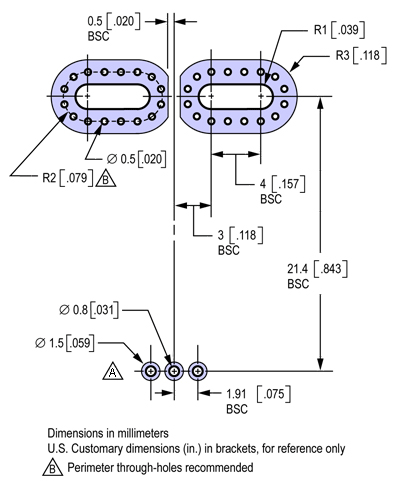
I'm trying to put a via on a slot hole pad (Package symbol level). But I don't have any idea on how to do it cause I'm kind of new on using cadence 16.6 

 This is the layout that I'm working on 

 layout

Thank you very much,

Borj 

PCB EDITOR 16.6 and 16.3 on the same computer?

$
0
0

 Hello,

        I just installed 16.6 on my computer under the assumption I could still launch 16.3.  16.6 is up and running as anticipated, however if I try to launch 16.3 I get the following error.

"The program can't start because cdn_xerces-c_2_7.dll is missing from your computer.  Try reinstalling to fix this problem."

 Did the install of 16.6 delete or move this .dll?  Should I reinstall 16.3?  Any guidance would be greatly appreciated.

Thanks,

Clint


Getting part on grid

$
0
0

I just loaded a netlist into a board where the default grid is set to 0.025". None of the parts came in on this 25 mil grid.

What is the trick to getting them on grid? (I hope it is not manually as there are over 700 parts............)

Tom

Preferred method of editing Orcad CIS parts database

$
0
0
I am looking for suggestions on what software I can use to modify part attributes that are in my Orcad CIS database.  For example, a resistor manufacturer has changed there numbering scheme.  So, I would like to open the database in a spreadsheet format and do a global replace of text for these parts.  I am using Microsoft SQL Server 2008 and I am not a database expert.  Just looking for an easy way to edit.

Allegro Design Entry CIS, schematic sheets disappeared!

$
0
0

I have no idea how come it happen, I just want to open my project, it opens for some reason in top bar saying (Read Only), and I see no schematic sheets! 

How come it be gone?


I'v browsed internet for that kind of problem, it was amazing to see that it is a "common" Cadence software problem for Capture schematic to be gone like that, and typical workaround is to add .dsn file by hand and it should work.

Well, I tried that, I click on Design Resources with right button, browse to .dsn file inside my project, and press Add, and nothing happens!

what has gone wrong?

This is really a nasty problem right in the middle of a project!!

Copper Pouring and Gloss (is it a problem?)

$
0
0

Hello,

i am designing a microcontroller 2 sided board in Allegro 16.5, after routing all the components, i want to apply the Copper Poring(Power Ground) on both sides.

I can do it easily but the problem is, after copper pouring when I use "Gloss" option , the blank spaces which was there between tracks and Copper pour vanishes and goes away. It looks like all the tracks got merged with the copper pour. This only happens when i use Gloss and i can not revert it back.

Is this only for the view or is it realy a problem? I am not able to figure it out.

a help will be appreciated. 


Difference between Symbols and Parts in Capture

$
0
0

 I am setting up a "site" capture.ini file and I noticed that there are entries for [Part Selector Configured Libraries] and [Symbol Selector Configured Libraries].  What is the difference between the two, because the entry paths don't typically seem to match.

Viewing all 5525 articles
Browse latest View live


Latest Images

<script src="https://jsc.adskeeper.com/r/s/rssing.com.1596347.js" async> </script>