Quantcast
Channel: Cadence PCB Design Forum
Viewing all 5525 articles
Browse latest View live

PSpice question: DC sweep family of curves

$
0
0

Hi all,

On academic network forum nobody could answer this question, so I hope this could be the better part of forum to post this question?

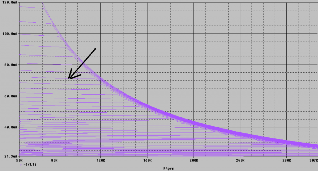
I make use of Primary sweep and Secondary sweep options in DC sweep analysis to obtain family of curves in Pspice. In my case I have two resistors: {R4prm} as primary sweep parameter, and {R1prm} as secondary sweep parameter. As a result of simulation the family of curves will be presented as illustrated on picture below.

Say I want to see what is the secondary parameter value for the specific curve (see the arrow pointing to curve on picture down there ). How can I do it, does anybody know? The cursor seems not usable for this purpose, it gives me only the primary sweep parameter value! 


Need older version of Allegro

$
0
0

I need to get my hands on version 15.7, or 15.5 Allegro.  Anybody know of, or have, a link where i can get a copy of the base release as well as the most recent ISR of the respective version?

Chad

Bluetooth RC Car

$
0
0

I am building a Bluetooth controlled RC car. I am a iOS / Android programmer, so that part is in the bag. What I'm looking to do is build a RC car driven with an Mobile phone. Are there any companies that would make me a custom PCB with a Bluetooth chip built in? What direction should I look to do research and what companies are good for mass producing custom PCBs? I've searched Google, but my problem is I don't know what terms to use to get the research started. I realise a post like this is gonna get tons of hate, but maybe one person out there will point me in the right direction.

Thank you. Simple design of what I'm thinking:

Plotting option is not get enabled?

$
0
0

Hi..

I want to plot the files of the corresponding board. When i am try to plot it with the asize or bsize , that time i can't able to plot it. can anyone provide detailed solution for the plot option

I had tried to search some tutorials too, but i can't find it. 

Capture CIS - BoM variant user property

$
0
0

Hello everyone,

I created BoM variants for my project using CIS. I want to generate the BoMs associated with each variant. 

I would like the BoM reports to display custom properties associated with the components. I cannot find a way to do this...

Can you please tell me if it is possible and how to manage such an operation?

Best regards,

Merwan Gacemi

Disks

$
0
0

Chad  - I have the original disks. Contact me via pm. Bill

Flash Symbols ("To Flash or not to Flash, that's the question")

$
0
0

Hi,

I would love some dialog about whether to use the Flash symbols for thermal relief or not. I have read a lot of material on the pros and cons and as Steve (local Pro around this forum), "why do the extra work?" I would seem that if its so critical and OrCAD teaching seems to go with the ideal of Negitive planes and pushes that type of design, then why wouldn't OrCAD just have a bunch of the flash symbols generic in the library and also have the padstacks setup with them in the layers?? In version 16.xx, if a Positive plane is selected, then the flash symbols are not used and you get the + across the pad so it just seems that the tools should have the padstacks defaulted with the Thermal Relief setup for Flash.

Any help shedding light on this subject is greatly appreciated.

KC 

Creating a custom Label for Footprint(dra)

$
0
0

Allegro has by default some Labels namely reference designator, value, tolerance etc., under the menu item Layout -> Labels -> Ref Des/Value/Tolerane etc. 

My question is How to create an Custom label, which takes values from schematic automatically as it does for Ref des and Value.

Thankyou.


Dynamic filled Planes go solid after a Constraints Manager change

$
0
0

Hi,

I have a 4 layer board with a power plane and ground plane. The xSection is setup as a "Positive" plane for both and connections to the power and grounds is correct and I have no DRC errors. I'm using OrCAD PCB Designer 16.6 with the latest patches or close (SP032). I've found that if I go into the Constraints Manager and change a property (i.e. Trace width, or a separation constraint etc. ) the dynamic filled planes go solid and of course then get DRC errors. I have to overcome this by going to the XSection and change to "Negitive" plane for power and ground and then Apply that change and then change back to a "Positive" plane and then the Ground and Power connections and etching is then correct. I've played with the Global Dynamic Parameters under <Shape> but still have the same problem. If someone can shed light on this issue, I would greatly appreciate your input. Seems like a bug in the tool but maybe I'm missing some setting.

Thanks.

KC

How to create "New Pin Number" by TCL Script

$
0
0

Dear All,

As the title, I create a new pin by tcl command " NewSymbolPinScalar " with class DboSymbol,

but when I run command " NewPinNumber ", there is a error occur : No matching function for overloaded 'DboDevice_NewPinNumber',

and the other command "SetPinNumber", was no use.

Is there any method to creat a new pin number by tcl command?

Thanks!

How to get pins' info from hundreds of dra files?

$
0
0

I've got hundreds of dra files and want to get pins' information( pad, pad's coordinate) from these files.
I've tried to record a script file(*.scr) to export pins' info as following:
1. open *.dra file
2. click "show element" button to look for pins' info
3. select all pins
4. save the information shown in the information window into a text file.
5. to parse the text file with python script to exact pins' info.

However, at step 3, I have to click the screen to do pick_origin job sothat Allegro can drag-select all the pins in a dra file.
For the hundreds of *.dra files, I've to click hundreds times! Not good, right?
Is there any shortcut or command to select all the pins?
Or can anyone show me another different way to get this job done?

Regards.

Route offset option in add command

$
0
0

I an using 16.6 .  How do you enable  the route offset to display in the options tab ?

Script to center refdes on parts

$
0
0

Is anyone aware of a skill script that can be run on refdes layers to center the text onto a part centers and at eith 0 or 90 degrees depending on part axis? 

Changing net on vias

$
0
0

Besides the traditional way to replace a via or reroute to it, does anyone know of a workaround or skill script to "assign" a net to a via much like we do with shapes? 

How to import the selected layers in the importing th .DXF file?

$
0
0

Hi..

I had worked on the four layer board with simple size. When i try to import the the layers of  Top, Bottom, Gnd, Pwr, OBS SSTOP , OBS SSBOT, drill,drill dwg.  the specific layers are not get selected.So i want to see above mentioned layers to view on my new .brd file. How to vanish the other layers that to be used in the .dxf file.The below the image is get attached.So any detailed solution for this problem.

    In case i try to remove it means that not get possible. Any idea to avoid this problem.


how to import the company logo on working PCB design?

$
0
0

Hi..

I had tried to place the logo drawn on auto cad & then tried to import it. But the result was not success. I am keep on trying to place the company logo in board, But i can't able to find the possible solution to this.

Any help for this problem?????

How to install the Logo maker on Windows 7 OS ?

$
0
0

Hi..

 I am trying to insert the company logo in the board file. For that i had downloaded the files http://community.cadence.com/cadence_technology_forums/f/27/t/13122 . In that i had download and install the precompiled potrace release.

My PC spec was Intel core 2 Duo with the 2GB RAM. But when i am try to install it, that time the cmd window is only executing. The software is not get executed.

So what version should be  downloaded  and what's procedure to install the logo maker with the potrace software. can anyone provide the possible procedure to install the logo maker.

After installing logo maker, Where it will be in PCB Editor?

$
0
0

Hi..

I had installed the Logo maker by the Dave's instructions and env variable path also been get changed and restarted the PCB Editor. Then i try to import the logo. Option is File----> Import------> What format i should use to import the logo maker option. I cant find the option. any help please....

 ca 

Try to fill copper area the filled area is moved certain distance

$
0
0

Hi.

 I had tried to filled the copper area for my board. Then in that case copper is filled through area where i want. In that the copper area around the pin is moved certain distance. 

I want to fill the copper fully filled with pin without clearance of pin. The image is attached below.

PCB Designer Does Not Update Screen

$
0
0

Changes mades on PCB appear (in real time) only in the world viewer. In the main screen the changes (as drawing a line) appears only after zoom is applied. I did not found a option to auto refresh screen.

Viewing all 5525 articles
Browse latest View live


<script src="https://jsc.adskeeper.com/r/s/rssing.com.1596347.js" async> </script>