Hello Everyone,
I am using Orcad PCB Designer Standard (version 17.2-2016 S065 [3/16/2020] Windows SPB 64-bit Edition) to design my second board and run into this Thru Pin to Shape DRC. Any help would be very much appreciated.
My board is a 4-layer board (signal/GND plane/PWR plane/signal). Whenever I add a shape (for copper) to enclose a thru-hole part on the inner plane (GND or PWR), I get this DRC on every pin of the part. The copper connects to all the pins and therefore these P/S DRC errors. Yet, when I add a shape in the same way on the outer layers, there is no problem. I did not run into this problem while working on my first board.
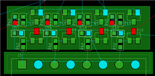
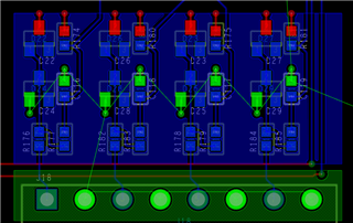
I am attaching two screenshots for your review with shape enclosed an 8-pin through-hole terminal block:
- Screenshot 1 with orange shape on the GND plane (with 8 DRC's)
- Screenshot 2 with green shape on the top signal layer (with no DRC)
- Screenshot 3 with green shape on the GND plane of my first board (with no DRC)
Please note that the second board started from scratch and not from the first board design environment/settings. I have checked the "Shape -> Global Dynamic Parameters..." of both files and they are the same.
What seems to be the cause

 ?. What other areas should I check?. Thanks.
TC