 Hi everyone,
Let me explain any one what is this rectangle ?? please clarify any one ??
Hi everyone,
Let me explain any one what is this rectangle ?? please clarify any one ??
Hi !
When I use Measurement function in Allegro, how could I see the measured length in both mm and inch simultaneously, in one same infomation window? Thanks!
generally , it can just indicate the Measurement result in one unit, either inch or mm. like following picture.

I have a resistor symbol set up to use a through hole footprint.
If I want that to be SMT, I have to manually type that smt name instead? It would be nice if I could assign a few different footprints, to my resistor symbol, and then just select.
Am I missing a basic feature that exists?
I enable the intertool communciation tab.
So I highlight the part in schematic but nothing got selectted in PCB editor
likewise I select the part in editor but nothing is highlighted in schematic
Inside the Editor, I used the Info button and clicked on the Via
It only shows it belongs to which Net.
No info on the type of Via is being used. No info on which plane its connected to.
So how do I find about more about a particular a via on a project?
Hi there!
We met a problem in place and annotate heterogeneous parts in hierarchy blocks.
An IC contains dual amplifiers, and it's schematic symbol consists of two heterogeneous parts(A and B).We use ONE amplifier in a specific hierarchy Block (name is BLOCK_TEST)
There are two Occurrences of BLOCK_TESTs in our project, so one IC is just enough. We attempted to place part A in BLOCK_TEST0 and place part B in BLOCK_TEST1.
There seems to be paradox: two BLOCK_TESTs is exactly the same occurrences, while the part A and part B is heterogeneous symbol.
How to solve this confilct?
The example dsn and olb file is attached.
Thanks very much!

(Please visit the site to view this file)
In design entry HDL, we have the check for "Wire is coming closer to the pin but no connected", like that do we have any check for two wires. In my case two wires are placed very closer (they meant to be connected), but because of grid issue they are not connected. Is there any feature to find this error???
In Allegro PCB , I created a symbol with mechanical mounting pins. I can place the Mechanical pins, but I can't delete them.
Edit --> Delete does not work.
Any ideas?
Any advice on modeling (spice) a brushed dc motor driver IC (drv8808a) for simulation within a ciruit? I have no idea how I would go about doing this.
hi everyone,
i tried to add the custom property for shape i could not add the property.in my design has nearly 500 shape presents.i need to convert the shape in to fill style should be Xhatch and void controls :Fill Xhatch cell should be high or low.i need to create custome property like that is it possible in
cadnece allegro ??
Hi, some days ago I have received a mail with the message that you find in the attached image.
Unfortunately changing from mils to mm, creates annoying errors in the DRC. This can happen, in to modify a board, that require symbols placed in mm.
I think that Cadence can resolve the thing, and to do better also !Please Cadence correct the thing, so that the competitors must keep silent !
I have forwarded this request also to the Cadence Local Partner.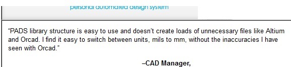
Hi,
Can any one explain how to change some ref designators(for eg some ferrite beads designators need to change FB instead of L without affecting inductor ref designators already present in schematics and board file) in Orcad 16.3 version?
Hello folks,
I tried to do apperently a simple thing but I get desperated. I need to mention that I am a beginner in Allegro.
I wanted to copy a part of a design (lets say clines and vias) to another. Therefore I created a net class including all nets of interest. With filter function "Find By Name" I chose my net class. All nets were highlighted but I am not able to edit them "Cannot edit Netclass ---.It is a logical group". When I set my filter by activating clines and vias and hover with the mouse over object of interest, select one ore multiple objects and try to edit them, it works perfectly. So I see, there is a differnce of selecting between these both methods, but how can I make this work? I would like just to edit the objects by selcting them over the net class. Maybe there is another way?
Could please anyone help me.
Regards,
Vick
Is there a way to use measure to measure from two points selected by the current cursor location ? For example measuring the size of a pad or anti pad opening ?
I'm trying to clean up some old schematics that drew parts from different locations, and hence have different formatting. I'm running into issues with how to make changes to entire pages or the whole design. The fixes are easy part by part, but there are hundreds of them. Many options seem to be unavailable when using the search function, like setting property visibility.
Thanks.
Hi all,
I want to export pdf file from a brd file with hatching format for shapes (left image), but Allegro just allows me to export as blank or solid shapes (right image). Anybody may give me a clue to solve this, thanks all.
I exported pdf with Allegro 16.6 lite in File -> export -> pdf (for both optional Filled shapes or not).
Hi everyone, Have anyone tried this company for circuit board manufacturing: www.pcbbasket.com
I have heard a lot of good comments about this manufacturing company. I am wondering, how was your experience with them, before I place my order. Quality really important for my product.
I just installed Allegro Free Physical Viewer v16.6 S002 on a new Desktop (Win7 Pro, x64, 8G ram). It takes minutes to load a brd file. Same file loads in ~10 sec on my 5yr old laptop, with only 6G ram, and while the laptop has other programs open, and the desktop has nothing else running.
I've tried uninstalling, cleaning the registry, reboot, and reinstall, but that doesn't help. Repeated that several times, with different number of registry cleaning before and after reboot. Also compared registry environment variables, and don't see anything that is different.
I've experienced before where a PC was "too fast" for a simulation software, and it would not find the license. Could this be similar? How then to slow down the PC to try? CPU is an i5-4590S, 3GHz, 3.3GHz turbo.
Appreciate any feedback and advice.
Thanks.
JKok
Hi all,
As I make changes from one version of my schematic to the next, I like to verify the changes by comparing the before/after netlist. However, Orcad is not consistent in how it lists the components. For example:
*SIGNAL* 12V_DRIVE
LC5.1 U1.8 R6.1 R7.2 R5.2 TP6.1 C4.1
See how the components are not in alphanumeric order? Without changing the net, the order in the next version might be different. So when I do a difference comparison, it shows a difference when the net really hasn't changed.
So, is there a way to force Orcad to output the components in a netlist in order? Or is there a tool designed for netlist comparison?
Thanks,
Paul
Hi everyone. I just got back my 2nd pcb using 16.6....so far so good. But I'm pretty sure I didnt use the best method for the soldermask so let me ask here. I did read through as much of the Orcad online help and manuals as I could but the pcb had to go out before I could seek out the best method.
I was requested that on some of the etch layer copper shapes....that parts of the soldermask needed to be removed. Not all of it....but some sections. So you'd have the shape most covered with mask but a few sections with exposed copper.
I did it by creating the shape needed by using the SHAPE ADD tool....and putting them on the BOARD GEO > SOLDERMASK LAYER. Then I included that subclass in the soldermask artwork.
After the pcb went out I read in the Orcad manual that was a no no....that filled shapes should only be on etch layers.
So what would have been the right way?
TIA!