Quantcast
Viewing all 5525 articles
Browse latest View live

STEP files not updating in board (but update in some symbols)

I'm having this weird issue - I'm trying to add connector heights so I can verify things with the mechanical engineer so I've been adding step files to my existing parts and some of them are updating and some of them aren't.  I've been using the STEP mapping from the setup menu and when I set up the offsets and orientations then save and refresh the package symbols some of them update and some of them are still not visible in the 3D view. 

I've tried updating the individual packages, all of the packages, updating the STEP mapping data only and ignoring the FIXED property.  I see the mapping information in the element information but I still can't see the STEP files in the 3D view.

I'm confused as to what to do - are there any debug logs or anything I can see?  All of the STEP files (the ones that work and the ones that don't) are all in the same place, all of the mapping files are in the same place and so far as I can tell the metadata is where it should be.  The step files render fine in the step mapping views so I'm assuming they're understood properly in OrCAD.  What else should I look into?

Thanks!

Chris

Image may be NSFW.
Clik here to view.

Quick place window not visible completely

Hi,

I am using OrCAD PCB 17.2 with hotfix 049. The quickplace window is not visible completely, the place and unplace buttons are not visible. I had raised an SR to Cadence regarding this, and it is in waiting stage from a long time. Has anyone come up with any solution for this issue? 

In my colleagues PC the same issue persists, but, when he hovers his mouse at the bottom the window, the quickplace window will scroll. How is it working in his system? Is there any settings to be changed in order to activate the mouse hover function?

Kindly help me with this issue.

Image may be NSFW.
Clik here to view.

How to change an attribute of a component group using console commands in Allegro Design Entry HDL

Hello,

Is it possible to change the value of an attribute of a component group using console commands? I am using Allegro Design Entry HDL version 17.2-2016.

Let's assume I want to change the HDL_POWER attribute of all power symbols from +3.3V to 3V3.

I found in the documentation the CHANGE command, but it allows me to do it manually on every component as far as I know.

Does anyone know how to do it?

Best regards,

Daniel

Image may be NSFW.
Clik here to view.

Can not open more then one board design in 17.2

Hello,

I am using orcad pcb designer professional 17.2 but I can't open two boards simultaneously. If one pcb design is open and I try to open another pcb board, I run into license problem and program does not open second design. I think I need to be able to open more board designs simultaneously. 

How can I solve the issue? 

Thank you in advance for your helps.

With kind regards,

Ahmet

Image may be NSFW.
Clik here to view.

17.2 Padstack Editor -- Opening scripts for 16.6 in 17.2?

Is there a simple way to open padstack scripts written for v16.6 in padstack editor v17.2? It seems like a complete scripting language overhaul. 

The root of this problem is that I exported a design from TI's WEBENCH tool. However the padstack scripts don't seem to work at all in v17.2. The first issue that occurs is "Can't find window; Form.padedit"

Here's a sample part of the script:

######################## New PadStack #########################
pse_new
fillin "R10180550000000A.pad"

FORM padedit units Mils
FORM padedit decimal_places 4

FORM padedit layers
FORM padedit grid row 1
FORM padedit geometry Rectangle
FORM padedit width 17.7165
FORM padedit height 55.1181
FORM padedit x_offset 0
FORM padedit y_offset 0
FORM padedit geometry_th Null
FORM padedit grid row 4
FORM padedit geometry Rectangle
FORM padedit width 17.7165
FORM padedit height 55.1181
FORM padedit x_offset 0
FORM padedit y_offset 0
FORM padedit grid row 6
FORM padedit geometry Rectangle
FORM padedit width 17.7165
FORM padedit height 55.1181
FORM padedit x_offset 0
FORM padedit y_offset 0
FORM padedit parameters
FORM padedit single YES
FORM padedit plating Non-Plated
pse_save_as
fillin "R10180550000000A.pad"

Here's a snippet from a script I started recording in v17.2:

# Pad Editor script
# file: 123.scr
# start time: Wed Dec 19 2018 16:35:30
# Version: 17.2 S033 (3691042) Windows SPB 64-bit Edition

QtSignal GuidedTabsParent PadstackTypes currentRowChanged 1
QtSignal GuidedTabsParent PadstackTypes itemSelectionChanged "SMD Pin"
QtSignal GuidedTabsParent PadstackTypes itemClicked "SMD Pin"
QtSignal GuidedTabsParent GuidedStartTab keyPressEvent 16777249 67108864 false 1
QtSignal MainWindow Units CurrentIndexChanged Millimeter
QtFillin Yes
QtSignal MainWindow Units CurrentIndexChanged Mils
QtFillin Yes

Image may be NSFW.
Clik here to view.

Database Manager in OrCAD Capture CIS

Dear all,

My problem is not create and modified my System DSNs in ODBC Data Source Administrator (using 32-bit).

[My Error: You are logged on with non-Administrative privileges. System DSNs could not be created or modified]

Likely, I predict that I can not choose my Data Source in Database Configuration in OrCAD Capture CIS 

[My Error: ORCIS-6245: Database Operation Failed Please Check Session For More Details]


Hope everyone needs help me.

Thanks so much!

Best Regards.

Image may be NSFW.
Clik here to view.

How to install old versions?

I'd like to install 17.2 S047.  How do I do it?  When I go to the download page all I see is the 17.2 base release and the hotfix to bring that to 049.  

Image may be NSFW.
Clik here to view.

Differential pair routing and setting vias correctly

Using Allegro 17.2

Are routing differential lines and need to change layer. Allegro sets vias but they will always be aligned horizontal in respect to each other and thus changing direction when routing horizontal.
I guess this is a simpel setting to correct but I cant find where. The image below describes the problem better than words. The orange arrow shows my routing direction when i click to set via. Then the vias are set as seen on the right image (marked wrong). What I would expect to happen is shown in the image to the left (marked "OK"). How do I accomplish this?

Image may be NSFW.
Clik here to view.

Breg

Vidar

Image may be NSFW.
Clik here to view.

I'd like to use the keyboard's "Enter" as a stroke or short key in pcb editor.

hello. I have a question. Please reply.

I'd like to use the keyboard's "Enter" as a stroke or short key in pcb editor.

I can't find a way. Don't you support it on PCB editor?

If there is any other way, please let me know.

thank you.

Image may be NSFW.
Clik here to view.

PSpice Co-Simulation ERROR(ORPSIM-2604): PSpice returned error. Terminating simulation.

Hello,

in SLPS CoSim, while simulating the demo files I am getting the error as shown below. please help to resolve this error

OrCAD version:17.2 hotfix : 049

MATLAB version r2017a

Image may be NSFW.
Clik here to view.

thanks,

Jesh

Image may be NSFW.
Clik here to view.

17.2HF049 capture part editor,move text/pin number/pin name can't snap to grid

17.2HF049 capture part editor,move text pin number/pin name can't snap to grid

and 

pin number/pin name can’t restore default location

Image may be NSFW.
Clik here to view.

COMPONENTS OVERLAP DRC

Hi expert,

There is special case that I have to overlap two components  to reserve two kind of footprint. 

I can understand the overlap DRC error on this case.

But there are still two other DRC type I do not know how to deal with.

One is rats: It seems just can be route/connect to one symbols pin while another one is can not accesible. So the rats exsit.

Am i should route all the two pins in different components? It seems i can not do it. How should I deal with this DRC error?

Another one is: Drill hole to line same net spcaing(because the footprint is dirllhole)

I guess this error is caused by the line and another pin which I do not connect.(I try to delete one symbols footprint and this DRC disappear)

How can i deal with this kind of error.

I think there are some cases that you have to reserve two footprint. Please teach me some about it. Thanks

Image may be NSFW.
Clik here to view.

Tab Key issue in PCB Designer 17.2.050

Hi all,

Since the update to the 17.2 version, I have been encountering an issue in PCB designer professional with the tab key which toggles the selection between the different selected elements of the filter. The software always reacts as there were more key stroke than one.I have found a workaround with the RMB menu and toggle select command, but it requires more clicks than the tab key stroke.

I hoped this would have been solved in the previous hotfix (050), but apparently not. This issue is not even listed in the CCR.

Do you also get the same behaviour? How can I submit a CCR by myself?

Thanks for your help and kind regards,

Nicolas

Image may be NSFW.
Clik here to view.

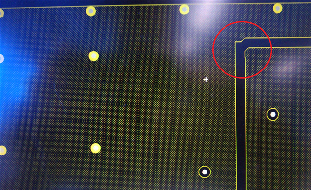
Shape edit boundary operation invalid

Hi expert,

I used to modify shape with Command "shape edit boundry" .

But sometimes I find this command invalid. 

For below instance, it is just a GND shape at GND PLANE.

When I using "shape edit boundry" command to modify shape vertex, it is invalid randomly.

I say it "random" because it can be work sometimes and it cannot sometimes.(I always try to operate on vertex point intentionally )

I can not summarize any rules between them.

My quesiong is:  Is there any special notice or regulation with this command which I have not aware it?

Image may be NSFW.
Clik here to view.

Image may be NSFW.
Clik here to view.

Hotkeys only occasionally working in pcb editor

Title mostly says it all, some times hotkeys work  some times not. Same edit modes, e.g., placement edit, having chosen a symbol, some times 'r' rotates the symbol and sometimes RMB and mouse moves seem to be be the only option. Would be very happy if someone could help shed some light, this seriously impacts work flow.

I'm using the latest version of professional. 

Image may be NSFW.
Clik here to view.

In DE-CIS/Orcad Tcl, is it possible to pass a parameter(filename) to an external binary?

The documented examples just don't address this.  I'm stumped.

exec command takes the path and filename of the binary provided I change from backslash to forward slash and double them up.

Why the documentation fumbles this, I just don't know.

I have conquered the task of exporting a list of part properties to a CSV file.

Just can't pass the path and filename of this CSV file to a VB script to do stuff like CIS DB queries

No error while executing
"exec "$lBinaryLocation""

What?  Sigh.

Image may be NSFW.
Clik here to view.

transient output file option in pspise

I want to save my simulation result in capture every 100us and export them in text file. I went to simulation settings>Analysis>output file option and changed print values in output file every 100us (my settings in orcad capture)Image may be NSFW.
Clik here to view.
but when my simulation time finished and export my result in text file Image may be NSFW.
Clik here to view.
Image may be NSFW.
Clik here to view.
time steps doesn't match to my setting in final text file. Image may be NSFW.
Clik here to view.
On the other hand I want to save my result in text file every 100us, how should I do this?

Image may be NSFW.
Clik here to view.

Allegro and SharePoint

My team wants to use Microsoft SharePoint for library storage.

Has anyone tried this?

Is there a way to have allegro to point to a sSharePoint  folder to load all the library files?

Many thanks in advance.

Wild

Image may be NSFW.
Clik here to view.

A symbol is placed into capture CIS,but pin name is not aligned.Symbol is edited by cadence 17.2. WHY?

Image may be NSFW.
Clik here to view.

Image may be NSFW.
Clik here to view.

Orcad Tcl_Create Library Part from Excel File using TCL

Hi Team,

Greetings!!

I am working  to write a tcl code to create the library parts and add the user properties from Excel file(eg., Resistor_olb.xls)

Image may be NSFW.
Clik here to view.

Against this Excel File I need to read the cells and create parts then add  User properties for that part.

Please advise how to achieve this.  Also I request you to  provide some sample tcl programs regarding this task. 

Thanks in Advance.

Regards,

dvk

Image may be NSFW.
Clik here to view.
Viewing all 5525 articles
Browse latest View live


<script src="https://jsc.adskeeper.com/r/s/rssing.com.1596347.js" async> </script>