I just recently started using the High-Speed/Miniaturization options with Allegro 172, and suddenly I'm experiencing crashing at least 2-3 times a day. The error message says "Program has encountered a problem and must exit...". In working with my support folks, I was advised to try disabling OpenGL. That fixed the crashing problem, but I like OpenGL because I like to see the netnames on my traces. After doing some research, I'm now questioning whether my graphics card (Intel UHD Graphics 620) is adequate for the High-Speed/Miniaturization option. Does it really required more graphics horsepower than I have? Has anyone else experienced this issue? Do I need a new laptop? Thanks for any guidance.
↧
Graphics Cards and High-Speed/Miniaturization Options
↧
Allegro 17.2 Desgin Entry HDL Error (SPCOCD-553)
Dear All,
I am newbies in the Cadence Allegro Design Software.
I am facing the error in the Allegro Design Entry HDL opening. Please find the attached Error for the reference. The Software gets hang after this error.
Please help me to resolve this issue.
Regards,
Mohsin
↧
↧
select entire net refresh in 17.2HF052 capture is very slow
Hi guy!
I found that select entire net refresh in 17.2 capture is very slow, and there will be similar unresponsiveness in the middle.
This problem mainly occurs when selecting GND or VCC.
I don't think it's a slow computer response. My computer hardware configuration is Intel i7 3.0 GHz, 8GB RAM, SDD.
In the same DSN file, I tried to refresh it very quickly in 16.6, which would not happen above.
I wonder if anyone else has encountered this kind of problem?
↧
[Capture CIS] Preview 3D model for database parts + more component details
Hello
Under Place Database Part in Capture CIS, Is there any way we can get a 3D preview of those parts which has a step attached to their footprint?

If not, is there any way to get a more detailed preview of the footprint than a green wire frame?
Also, would it be possible to see description of the component in a viewing window like this:

Best regards
Mysil
↧
OrCad PCB Editor File Extensions - a definitive list *please*
In the process of creating footprints, board layouts, format symbols and the like, OrCAD PCB editor creates a plethora of files and some sub-folders.
We have a repository and want to save out ONLY the files we NEED to save instead of this maelstrom of files and folders.
I have been looking for a definitive list of file extensions used by or generated by OrCAD PCB editor so that I can determine exactly which files we MUST save and which may be discarded.
e.g. A PCB footprint requires a *.DRA and a *.PSM file. All other files may be discarded.
Can anyone help me with such a list?
↧
↧
Creating paste stencil with both sides in one stencil
Hi
So I have a bit of a weird question; I'm trying to create a single stencil with both sides of my PCB on it (this is because my stencil manual printer basically has a minimum size and my board is tiny) so from looking around the way I'm trying to do this is to export one side's paste mask as an IPF then import it; mirror it and export the combined side as a single larger gerber which I then can upload to the stencil creation site. The problem I'm running in to is that the imported IPF is an outlined version of the other side so the stencil only has half of the details as necessary (since the other half is just infinitesimally thin lines outlining the shapes) - are there any recommended ways to do this? I'm thinking either if I can import the IPF as shapes that are filled rather than outlines (not sure if this is possible) or something else entirely.
Thanks!
↧
converting a text into a polyline on dxf export
hello
is there any way i can convert a text to a polyline when exporting a design file as a dxf file?
↧
Bend operations disabled due to licensing and/or DLL installation issues
Hello All,
After the installation of the latest Hotfix_SPB17.20.053_wint_1of1, I get an error message in 3D canvas:
Bend operations are disabled due to licensing and/or DLL installation issues
Is there a solution except waiting for the next hotfix?
Anybody has an idea how to rollback to the previous one?
Thanks in advance and have a nice day.
↧
Advice on moving forward. (I believe unit's of measurements caused an issue)
I've posted about this a few weeks back, but work has been hectic, and I haven't had a chance to work with ORCAD since. Here is what's going on. I have two boards that have 30 pin connectors, which have become obsolete. We chose a new one, and I got to work making the changes to the board design. The first board is complete (but being reviewed by someone for me by the company handling the prototype), but when I went to make the changes to the second board, I ran into major issues. The second board only had one change to make( board #1 had 5). This change uses the exact 30 pin connector that was changed on board #1.
When I replaced the footprint on board 1, it simply replaced the old one and broke several connections related to the pins of the connector. Some simple routing fixed it up in not much time at all (when I figured out what I was doing).
I was expecting the second board to be done in one afternoon because it required much less work. To my surprise , replacing the connector on this board, created havoc. There are ratsnests EVERYWHERE. So many connections are broken, that it will take me forever to fix it.
After doing some digging around, I found a possible cause. Board #1 used one unit of measurement, and board #2 used another(made by different companies), from an old post I found on the forums. The fix recommended on this thread didn't work for me at all, so now i'm wondering what my next move should be.
Should I just remake the footprint, using the same units as the board? Or should I change the units of the board to match the units of the footprint? Is there an even better option that I haven't considered? Or have I done something else wrong entirely?
↧
↧
Creating an alternate sch symbol for a multi piece component allegro HDL 17.2
We have a part number, SEAF-40-06.5-S-10-1-A-K-TR in our system. It is a connector and has 4 parts (that are listed as variants) to it. The way it was laid out pin wise was bad. However its already on some schematics so we can't just delete it. So without having to creatively make another p/n how can we have an alternate set of sub parts to this component?
Thanks,
Charles
↧
DRC ERROR
Hi everybody,
I'm writing because I would like ask to you a suggestion about DRC.
For examle: I have a net ( It is a shunt) with an min line width of 1 mm. I need to read the current so I have to take the signal an to go to comparator. The part of net that go to comparator is 0,2 mm ( it hasn't to be1 m) and correctly i have DRC error.
Do you know a way for not have this error only part of small net? Do you have any suggestions?
Thanks.
↧
Refresh Capture.ini without restarting Capture?
I have this in my CDS_SITE Capture.ini
[Part Library Directories]
Dir0=C:\Cadence\Library\Logic
This will load all the OLB libraries within Dir0 when Capture opens. Is it possible to reload it if a library changed or was updated without restarting Capture? The library exists on disk, just Capture was not configured on startup. If you try to place the part using CIS you will get this error:
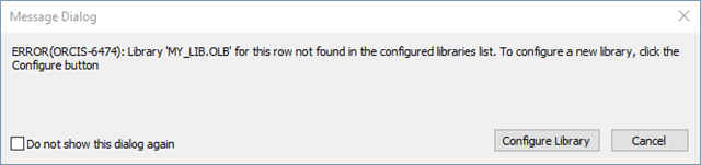
If you browse to the "my_lib.olb" library and select it everything works fine. But it would be nice to refresh all libraries at once.
Thanks for any advice!
↧
Differences between a netclass and a netgroup
Hi ,
I am trying to figure out the differences between a netclass and netgroup in constraint manager. Can anyone explain when you would use one or the other ?
↧
↧
failure of creating net list
Hello, i just started PCB designing in cadence 16.5, ORCAD capture. I draw the schematic in capture and i created my own footprint for package and uploaded the footprint in property, define the pins in symbol and selected the path for .dra, .psm and .pad files but when i proceed for the creating Netlist it takes long time "~30Sec" and a massage pop up saying " pstswp.exe stopped working" and net listing failed and their is no error in session log.
.in this schematic i had done some changes in the symbol pins " i defined some pin by PACK_SHORT". Before this updatation the Net list creation is successful and PCB editor board is uploaded but after these changes their is error in creating Netlist. does any one has a solution of this problem??..
↧
square shaped void with radius
hello
how can i change a square shaped void on a shape to a void with a radius at 4 corner?
↧
copying a void to a shape on another layer
hello
how can i copy a void on a shape on Layer 1 to a shape on Layer 2?
↧
offsetting a void shape
hello
how can i offset a void shape?
for instance, i want to make a 40um square shaped void a 30um square shaped void.
↧
↧
Thur Pin and Via clearance to shape/plane disappear
Hello all together,
I'm staring to learn Cadence (capture CIS and PCB Editor) and at moment I'm lost with a strange problem I couldn't figure out by myself - even after extensive web research and tutorials.
I skipped using a Plane layer, because I found in this forum its hard for a beginner, so I started to switch all layer form "Plane" to "Conductive", which means "positive" WYSIWYG design. I'm OK with that.
Now I started to draw shapes to define my GND planes as dynamic copper and allocate my GND net.
But all VIA and Thru Pins behaving very strange.
- when only less then a half of the circle is covered by the shape, a "anti etch" area appears with the clearance defined in the CM.
- but when more than a half circle is covers by the shape, no clearance appears and the DRC is marking a failure.
- also the GND pins will not connect to the shape in the way defined in the global Shape Thermal connect settings
What can I do to avoid this behavior?
I started to check all CM settings, but maxbe I missed sth?
Thank you very much!
Andi![]()
↧
why line to SMD Pin same net spacing DRC?they are one the same net.

↧
Testprep Automatic - allow pin escape insertion function - doesn't work as expected
Hi all!
I'm trying to add as much testpoints as I can on a board that has ~380 nets. In the ideal world, I'd like all my testpoints to be located on the bottom layer. In order to accomplish this, I'm trying to use the "Testpret Automatic" support from OrCAD PCB (I'm using OrCAD PCB Designer Professional v16.6 S069), after having set my testpoint to component location constraint in the constraints manager modes.
I have set the parameters (Testprep Parameters dialog) to have the test points on Via pin type only; SMD/Blind; Bottom layer and Single mode; no test grid restriction (0, 0); I haven't checked the "Disable cline bubbling". On the Padstack Selection I have selected a valid "SMT Testpad", which has a pad on the bottom layer only in the padstack and selected a "Thru Via" which I use (among others) in the design. I have also one probe type enabled, with which I want to have a minimum clearance of 2.0mm between the test points.
In the Testprep Automatic dialog, I check "Allow test directly on trace" and "Allow pin escape insertion" and set the maximum via displacement to be 3.0mm. When I run the "Generate testpoints", I get around 120 test points generated, but not according to my expectation. The test pads (vias) that I get are put on one of the three positions:
1. Ether on a track (in the middle);
2. Close to a pre-existing via, and connected to it with an autoplaced cline - the same type as selected in the "Thru Via" field in the Parameters dialog
3. Close to a pre-existing via, and connected to it with a cline, but the via is some other one that I use in the design.
According to the documentation, regarding the Allow pin escape insertion:
"In conjunction with the Thru via field on the Padstack Selections tab and theVia displacement fields, automatically adds an SMT test pad and a via to a net if no suitable test site exists. Use this option for in-circuit tests to ensure top- or bottom-side access to all surface-mount-technology devices or for routed nets without through-hole vias. Routing is added despite the presence of a NO_PROBE area that may be placed over pins. The actual via is placed outside the NO_PROBE area. When locating a via outside a NO_PROBE area, the Via displacement: Max parameter setting controls the distance allowed from the pin to go beyond any NO_PROBE area. Allowing pin escape insertion requires a route keepin."
I expect to get an extra via connecting a trace on the Top layer, to a testpin on the bottom side. I don't get this, and just have all the connections made to pre-existing vias on the board.
I have played around with different grid sizes on the Etch layers, as well as different displacement Min/Max values for the testprep vias - I still didn't get new vias connecting the top layer nets to the bottom one, so that a test via can be added. I read on couple of threads here that dynamic shapes can sometimes interfere with the pin escape insertion function - so I removed all the dynamic shapes (saved them to a sub drawing for later to be imported back), and re-run the automatic testprep, with the same parameters as stated above - again no new vias were added, and only connections to existing vias are made.
Have I miss interpreted the documentation (if so, please correct me), or am I doing something wrong with setting the parameters?
Please find the pictures of all the setup dialogs on the following link: https://imgur.com/a/T7QtYU1
Thanks a lot for any assistance!
Cheers,
Aleks
↧