Quantcast
Channel: Cadence PCB Design Forum
Viewing all 5525 articles
Browse latest View live

Netlist property syntax warnings after back annotation, then netlist re-import

$
0
0

My toolset is OrCad PCB Editor 17.4-S009.

I recently performed a back annotation from PCB Editor to Capture, then re-generated a netlist in Capture to import into PCB Editor (to be sure they are synced). When I imported the netlist into PCB Editor, I have the following new warnings:

------ Oversights/Warnings/Errors ------

#1   WARNING(SPMHNI-316): Property warning detected.
WARNING(SPMHNI-217): Problems with net 'D1_MA11'. Error with net property 'RELATIVE_PROPAGATION_DELAY' and value 'MG_DDR4_ADDR_5:G:U16.N2:U21.N2:::MG_DDR4_ADDR_4:G:U9.N2:U16.N2:::::': 'expected syntax is <group>:<scope>:<pin1>:<pin2>:<delta>:<tolerance>'.
#2   WARNING(SPMHNI-316): Property warning detected.
WARNING(SPMHNI-217): Problems with net 'D1_MA2'. Error with net property 'RELATIVE_PROPAGATION_DELAY' and value 'MG_DDR4_ADDR_3:G:U6.M3:U9.M3::::': 'expected syntax is <group>:<scope>:<pin1>:<pin2>:<delta>:<tolerance>'.
#3   WARNING(SPMHNI-316): Property warning detected.
WARNING(SPMHNI-217): Problems with net 'D1_MBA1'. Error with net property 'RELATIVE_PROPAGATION_DELAY' and value 'MG_DDR4_ADDR_6:G:U21.K8:R131.1:::::::': 'expected syntax is <group>:<scope>:<pin1>:<pin2>:<delta>:<tolerance>'.
#4   WARNING(SPMHNI-316): Property warning detected.
WARNING(SPMHNI-217): Problems with net 'D1_MCK1_B'. Error with net property 'RELATIVE_PROPAGATION_DELAY' and value 'MG_DDR4_ADDR_6:G:U38.F8:R136.1:0.00 MIL:5.00 MIL::::MG_DDR4_ADDR_2:G:U31.F8:U33.F8:::MG_DDR4_ADDR_1:G:U5.AC29:U31.F8::': 'expected syntax is <group>:<scope>:<pin1>:<pin2>:<delta>:<tole

I performed a DBDoctor update through the external application with no change. Any idea on how to resolve? Prior to this, I had no DRC errors at all.


RMB Customize Enable Single Click Execution

$
0
0

This is enabled by default and is painful to me. How can I disable this by default?

Integration with version control system

$
0
0

Hello everyone.

I have been using OrCAD for more than a year now and I think about implementation a version control system. 

So far, I have used gitlab for symbols and footprints and I didn't expect it to work so good. Although symbols are stored in binary files, Gitlab handles them with no problems. There is no issues with creating symbols, pushing and merging. No conflicts at all. Additionaly, I share the libraries with other co-workers. Everyone is capable of commit. That's a plus for Cadence.

But how do you manage your schematic and layout files? Is it any way to do it? I have enough of creating a copy once an hour or more often. 

What's your experience in that topic? What do you think?

Error SMD pad not 'Either' layer for the 'Test SMT/blind pad'

$
0
0

Hello,

 I'm working on a pcb revision of a master.

I received the database from the custumer and I don't know who designed the previous release.

Evertime I pick a new track on log windows appears this message

Error  SMD pad not 'Either' layer for the 'Test SMT/blind pad'

I tried on Design Parameter Editor but I can clear this error.

Some ideas?

Thanks

Stefano

How to generate artwork film with drill symbols from a specific via type?

$
0
0

I want to output an artwork film showing the via in pad locations. All the via in pad locations on my project use the same via that has a unique drill diameter. 

How do I go about generating an artwork film that shows only this via symbol while ignoring all other via symbols?

My toolset is OrCAD PCB Editor 17.4-S009.

Use of LibreOffice versus MS Excel for Capture BOM Creation

$
0
0

Folks,

Had this discussion sometime back on the forum, but am I the only one who does not want to continue paying Microsoft for their Office Suite when there exists many open-source office suites.  Most notable among them is Libre Office.  Would be nice if Capture could also "look" for LibreOffice's Calc and not just MS Excel through the API call.

Thoughts, people?

Chris

more PCB in one brd.

$
0
0

Hello,

In my design I have two PCBs in one BRD file. This is why I want to adapt this two board mechanicaly.

I can't use Design_Outlines two times. I can use for example two Outlines, but in this case I can't use the 3D Canvas.

Everybody know how is it possible to create one brd. with two PCBs?

Thanks

Allegro fanout ratsnest connection to ground plane lost after footprint symbol update, but tracks present

$
0
0

Hello,

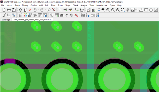
In Allegro 17.2, I previously had fanout connections to a ground plane for a QFN footprint with no more unconnected ratsnestlines. I changed the footprint symbol and did an update. All over at the connections to the ground and 1.8V power planes I see ratsnests appearing between the pins as if the fanout connections were not there. However, the tracks are still there. (see the picture for pins 12 and 10) To make the ratsnests dissappear, I have to delete the tracks and fanout again.  How come? Can I reconnect the tracks automatically?

(I enabled the display design parameter to show the holes and have the ratsnest geometry set to straight)


new device CLASSes ? in capture.

$
0
0

Hello there.

 I came across this message in capture:

CLASS property 'NONE' is illegal: 'Class must be one of IC, IO, DISCRETE, MECHANICAL, PLATING_BAR or DRIVER_CELL.'.

Of course is obvious that I can't assign NONE as class but I have never know about those classes:
MECHANICAL, PLATING_BAR or DRIVER_CELL

What is their use?

Regards

Krissn

overlapped Vias with the same net - How to create a rule to find the vias

$
0
0

Hi to all,

I' m working on PCB that I have got from another collegue.

I have an little request: I have overlapped some vias with the same net.

What I can do is to create an proper rule in constraint in order to find this vias and delete one of them

Can someone help me?

mY orcad is 17.4 2019

.

Schematic capture modification

$
0
0

We tie schematic capture to our parts data base for all of our parts. We are now trying to add some extra fields to this list. The first picture shows the area we are trying to change. The second picture is the capture.ini file that shows the column count is = 35 which is shown in picture 1. We have tried making changes but it seem to be limited to only 35 columns. We tried to add more but it doesn't change. We tried renaming some of them and they either moved to the end of the column or didn't change.

So is 35 the limit or can we add more columns or is there something we are not changing that will let us add more columns. 

Etch Shape only Keepout?

$
0
0

Is there a keepout (or other method) that allows clines and vias in the area, but does not allow etch shapes? The goal is a permanent etch shape keepout, so shape voids are not the solution.  Thanks for any help you can provide. -lou 

Double clik con DSN starts PCB Ruoter

$
0
0

Hello,

 I installed 17.4

Before installing it with a double click on DSN started Capture 17.2

Now stars PCB Router and not Capture 17.4

I tried with windows "Open with" in context menu but starts always PCB Router

Any idea?

Thanks

Stefano

Problem generating PDF of Assembly Drawing

$
0
0

Hi 

I am trying to export assembly drawing of my layout with Package Geometry>Ass Top and Components>Ref DES Options.

But i cannot manage to change the page layout to Landscape mode. I have tried several options including:

Print Preview> Layout. Nothing happens after i press Layout.

If i choose Print Preview> Print. Even after i choose Landscape Mode it prints out pdf in Portrait mode.

 It has worked before well but after a hotfix update this issue started.

Assembly drawing , allegro

$
0
0

Hello all ,

     I'm using orcad  17.2 . Try to export -variants- create assembly drawing  in orcad  . But it shows variants.lst file not found . How to overcome this . Anyone kindly explain details... 

Thanks & regards ..


Accurate trace width simulation

$
0
0

Hello everyone

I wonder if there is a way to simulate the accurate width of a pcb trace depending on the flowing current.

Thanks in advance.

What the heck happened to ratsnest during move?

$
0
0

I noticed a few releases ago in 17.2.xx that rats stopped showing during move even tho ripup was selected.  Then in 17.4 same thing.

Did a setting change or did some beginner at Cadence decide this was a useless function?

ADJACENT_LAYER_KEEPOUT_BELOW not working in 17.2 ?

$
0
0

Hi Everyone,

i set the  property for pin  ADJACENT_LAYER_KEEPOUT_BELOW but i could not find any route keep out in below ground layer. Can any one solve this issue. ?

Thanks 

Kabaleeswaran.K.R

Resizing DXF file

$
0
0

Hello everyone.

I want to add a logo of my company to a PCB board.

At first, I converted a PNG file into a DXF file not to lose quality and imported it into OrCAD. I create it as a mechanical symbol.

Everything seems to be good except dimensions. The image has dimensions of 2000 x 1000 mm. Is it possible to resize the image without losing quality? 

I tried to resize a png file and then into a DXF file, but the quality is awful and that didn't work.

For now, I've imported a DXF file that has big dimensions.

Create shape from lines (compose shape?)

$
0
0

Hello,

 I've a board with complex outline

I loaded DXF file on an unused graphical layer.

I changed to Design Outline.

Now I've to z-copy this outline for package and route keepin, but z-copy needs a shape.

If I use the command Create Shape From Lines the shape is filled and I can get simple shape-outline.

What's wrong? I found on forum some thread about the command "Compose shape" but I think I was on older version of Orcad.

Any idea?

Thanks

Stefano

Viewing all 5525 articles
Browse latest View live