Quantcast
Channel: Cadence PCB Design Forum
Viewing all 5525 articles
Browse latest View live

Allegro Constraints Manager values

$
0
0

 I want to set the minimum and maximum width

conductors (Line Width: Min / Max), the minimum width and
the maximum length of the places of attachment to the conclusions / transitional
holes (Neck: Min-Width / Max Length) and gaps in/out point and
the length of the differential pairs (Differential Pairs).
But the calculator  http://circuitcalculator.com/wordpress/?p=25/ of these values gives only the width of the conductor. How to get the other options ?
 

DboTclHelper_sCloseCFile returns "RuntimeError..."

$
0
0

Hi Sir,

    I tried to use DboPage_CopyToFile and DboPage_CopyFromFile, and those two procedure need CFile* argument. There are two functions in DboTclHelper about CFile: DboTclHelper_sGetCFile and DboTclHelper_sCloseCFile.  But i can not get any information about how to set FileMode (in sGetCFile), and after called CopyFromFile and then sCloseFile, it will return a Error: "RuntimeError unknown exception", this error will cause Capture crash.

My Question:

1. How to set the FileMode argument (read/write/append/.... )?

2. How to close CFile* gracefully?

     Any document about those functions will be appreciated.

     Thank you.

Daniel 

[PCB] Create solid shape in silkscreen?

$
0
0

Hello,

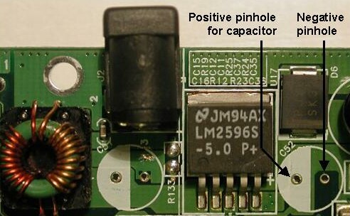
I want to create silkscreen for capacitor like some commercial board that contains the solid circle (see below). The silkscreen generator (AutoSilk) can't generate the shape. What should I do?


Thanks for your help.

Importing .TEL netlist and library search

$
0
0

 I can import a netlist from Orcad and it searchs all the library directories for symbols. When I import a other netlist (.tel) the symbols all need to be in that same directory as the .tel file. How can I have it search all the library directories ?

New VIA definition

$
0
0

Hi!


I have to you the following questions:

1) How do I define the new VIA so that I can use it later in Allegro? I know that I have to use the  PAD Designer, but where I have to save the designed VIA so it is later visible in "Edit VIA List" within Constraint Manager in Allegro?

 2) How I add to the layout a single VIA e.g. if I want to connect two planes together that are on different layers?


Best regards,

Krzysztof Sielewicz 


Kitchens Cabinets London

$
0
0


Normal 0 false false false IN X-NONE X-NONE /* Style Definitions */ table.MsoNormalTable {mso-style-name:"Table Normal"; mso-tstyle-rowband-size:0; mso-tstyle-colband-size:0; mso-style-noshow:yes; mso-style-priority:99; mso-style-qformat:yes; mso-style-parent:""; mso-padding-alt:0cm 5.4pt 0cm 5.4pt; mso-para-margin-top:0cm; mso-para-margin-right:0cm; mso-para-margin-bottom:10.0pt; mso-para-margin-left:0cm; line-height:115%; mso-pagination:widow-orphan; font-size:11.0pt; font-family:"Calibri","sans-serif"; mso-ascii-font-family:Calibri; mso-ascii-theme-font:minor-latin; mso-fareast-font-family:"Times New Roman"; mso-fareast-theme-font:minor-fareast; mso-hansi-font-family:Calibri; mso-hansi-theme-font:minor-latin; mso-bidi-font-family:"Times New Roman"; mso-bidi-theme-font:minor-bidi;}Kitchens Cabinets London, Thirty Ex Display Kitchens To Clear. www.exdisplaykitchens1.co.uk£ 595 Each with appliances.


[URL=http://www.kitchenslondon-kitchenslondon.co.uk]Kitchens Cabinets London[/UR


Kitchens Cabinets London

$
0
0


Normal 0 false false false IN X-NONE X-NONE /* Style Definitions */ table.MsoNormalTable {mso-style-name:"Table Normal"; mso-tstyle-rowband-size:0; mso-tstyle-colband-size:0; mso-style-noshow:yes; mso-style-priority:99; mso-style-qformat:yes; mso-style-parent:""; mso-padding-alt:0cm 5.4pt 0cm 5.4pt; mso-para-margin-top:0cm; mso-para-margin-right:0cm; mso-para-margin-bottom:10.0pt; mso-para-margin-left:0cm; line-height:115%; mso-pagination:widow-orphan; font-size:11.0pt; font-family:"Calibri","sans-serif"; mso-ascii-font-family:Calibri; mso-ascii-theme-font:minor-latin; mso-fareast-font-family:"Times New Roman"; mso-fareast-theme-font:minor-fareast; mso-hansi-font-family:Calibri; mso-hansi-theme-font:minor-latin; mso-bidi-font-family:"Times New Roman"; mso-bidi-theme-font:minor-bidi;}

Kitchens Cabinets London, Thirty Ex Display Kitchens To Clear. www.exdisplaykitchens1.co.uk£ 595 Each with appliances.


How can I preserve designators from changes?

$
0
0

Hi
In the Orcad capture schematic environment when we try to copy a page in a project file and paste it into an another project all designators automatically changes.
How can I preserve them from changes?
It is important to me to save all designators without changes.
Thanks a lot


How to Place Components without Dimension Information

$
0
0

Hello all,

I'm having difficulty locating the function that will allow me to place components without dimension information about the footprint. This wouldn't be a problem if my computer isn't so slow and I didn't have 150~ parts in my design. My computer will often freeze when PCB Editor decides to display footprint dimensions for every 0805 resistors / capacitors or soic8 ICs.

Thank you for your time,

Andy Park 

Is there a way to generate a color map/chart to assist in assembly?

$
0
0

Our normal process for manual assembly is print out the assembly drawing, the assembler colorizes the assembly drawing so he can easity identify where the parts go, i.e. 100 ohm resistors are red, 50 ohm resistors are blue, the opamp is green, etc.

 Does Allegro have a built in function to color code parts based on part number?  If not, I think it would be a nice addition to the PCB capabilities as it can save me hours of time.

Design Entry HDL Hierarchy Viewer empty

$
0
0

I am using design entry HDL  v16.6 with the newest hotfix. I have been working on a schematic and the hierarchy viewer had the schematic name and the pages listed. I was trying to fix some installation and license issues and in the process I made my hierarchy disappear. Not the viewer, but its contents. I tried to go back through what I did but couldn't remember everything. Even though nothing appears in the viewer, the pages in my schematic are still there and I can scroll through them with the page up and down keys or go to page.

I have tried right clicking and choosing "show pages" but nothing happened. and I have tried closing and reopening the project.

I attached a screenshot of my present schematic and from a new schematic that displays properly. 


Thank you.


Other potentially relevant info:

-I now get this error when I open the schematic "INFO(SPCOCN-245): Unknown project directive : #TEXT_EDITOR."

-I created a new project/schematic and it works correctly, no error, hierarchy is there.

Vias in Symbol

$
0
0

All,

Thsi poat is re-visited because I couldn't make it work the last time and had to kluge my way through my design. My situation is that I have a FET with a large pin. I need to add an array of 30(6x5) vias in the symbopl on that large pin to use as a thermal array. There was several suggestions but I couldn't get these to work and had to move on. I'm back asking for advise. Any hints will be helpful as I am am coming up on schedule.I'll attach a screen shot that will show the problem.

Thanks,.

Ron Scott CID+

ron.scott@halla.com 

Creating a model in pspice model editor

$
0
0

Hello all,

I am new to the using of the pspice model editor, Can anyone help me in giving a brief idea regarding  how to model a NEMS switch based on its I-V characteristics.


Please help me in this regard

Thanks

Revanth Rajalbandi 

Upgrade from Orcad Capture 16.0 to 16.6 library incompatible

$
0
0

I'm runing Orcad Catpure 16.0 and I'd like to upgrade to 16.6 but the libraries don't seem to be compatible.  Does anyone know what the process is to do this? 

 Also, can I open a 16.6 schematic file and save it in 16.0 format?  

Thanks in advance. 

RF Designe basic calculations like Why we place the Capacitor............?

$
0
0

Hi All,

         I'm PCB designer as if now working on RF card.  I have some doubts in RF Design.

1. Why we place Capacitor or inductor in path of Antenna . If required how to calculate the value of Capacitor or inductor.

2. How we need to calcutate the length of trace between antenna to IC .(i.e will  Depending on the Frequency or what).

3.Please let me know any basic refrence book or site for RF design Basics.

Any Help will Appreciated .

Thanks in Advance.!!!!!!!!!!!!!!!!!!!!!!! 

Good Day,

Pavan Kumar 


how create a ".cir" file in Orcad 16.3

$
0
0
Hello, 
I would like to create a "cir." file in Orcad 16.3 but I'm a little lost, is that you can help me? 
is and what you can tell me how to change the number of output bipolar transistors, ie, I find in the software transistors 3 terminals (EBC), while I want to add the substrate channel but I do not know how. and when I change the netlest and I run the simulation it removes all the changes I did. 
Thank you for your help.

PCB editor name/versions?

pxl.exe has stopped working

$
0
0

When I try to export physical, I get a windows error box that says "pxl.exe has stopped working". I click close the program a Design Sync error shows "Error: PXL Failed. Unable to package the design. Do you wish to view the pxl.log file?" If I click yes, it fails to open the documents, presumably because it was never generated. I saw an article that said this could be cause by having multiple paths in the $path environmental variables. I looked and didn't see anything but did a system restore to the last time that it worked anyway. It did not fix it. 


Any ideas?

[ALLEGRO] VIA-IN-PAD placement

$
0
0

Hi!


I have the question regarding the VIA-IN-PAD. How do I put the VIA in the BGA PAD so it is directly in the PAD center (when doing the BGA fan-out)?


Best regards,

Krzysztof 

Cross-Probing

$
0
0

All, 

I have been trying to get cross probing to work with less than favorable results. I have AppNote from EMA and have been exchanging posts with the AE. In a previous life, I had cross-probing working just fine. I followed alll the instructions but it seems the system is mute. I selected ICT in Capture CIS and made sure I ran a new netlist and set OrCAD  PCB Designer in highlight mode. No go. I then placed the schematic and layout in a folder on the C drive because the AE says it has a hard time across networks. No go. The last thing is the AE has no problems with the files I sent, I'd like to get this thing going for my user's sake. I don't really use it but now that's known it exists I should be able to offer cross probing to my clients/colleagues. Any help will be apppreiciated.

-Ron Scott 

Viewing all 5525 articles
Browse latest View live


<script src="https://jsc.adskeeper.com/r/s/rssing.com.1596347.js" async> </script>