Quantcast
Channel: Cadence PCB Design Forum
Viewing all 5525 articles
Browse latest View live

Artwork files generation the silk screen file are not enbaled??

$
0
0

Hi ..

I had finished the board, then i used to generate the artwork files for the corresponding board, that manufacture--->Artwork. In that the board outline, SST, SSB, SMT, SMB, Film mask  & Paste mask layers are not get enabled. What is the option i had to enable it.

In such, i had tried that add option, but the file is asking to browse the .txt file. What is it.??? How do i generate the artwork layers for above mentioned layers.


Dynamic Shape out of date, but not accessible.

$
0
0

Hi All,


I'm almost finished with my very first board layout using Allegro PCB editor 16.6 (latest hotfix June 2014), and I'm trying to generate the artwork so I can check over it and make sure it's good to send out to manufacturing. I'm having a problem when I try to create the artwork. It tells me that "Dynamic shapres are out of date; please update them. Check for out of date shapes in Setup Drawing Options dialog."

I look for the out of date shapes, and it tells me I have 1 dynamic shape that needs updating. I read that I could find out which was the offending shape by going to Display -> Status, and then clicking on the coloured button where it says "Out of date shapes." This then brings up another window. (see attached image)

As you can see from the image, the co-ordinates of the shape are way outside the limits of my drawing, and when I click on them, it tells me it cannot find the shape because it is outside the extents of the window. It is the only dynamic shape I have in my design now, as I have deleted the other 2 dynamic shapes ( GND and PWR planes).

How can I resolve this problem, and successfully generate the artwork I need? 

Capture - Edit Properties

$
0
0

I went on an Orcad capture course about 4 years ago but have only started using it this week! I'm seem to be running 16.6.

I have added several properties to library parts, and when I view these with "Edit Properties" on instances of the part within Capture, most (but not all) of the properties are displayed with a hatched background.

Why are they hatched? (Why are some I've added not hatched?) Can I turn the hatching off - it is harder to read. 

Creating new .brd with different netlist.

$
0
0

 A colleague and I started out with the same schematic but different blank boards. A minimum of parts were changed on both schematics; one type of FET on each board. I built the physical symbol for each new FET and put them in the library. I am able to put both FETS on my variety of the board but on my colleagues board; I can't net on his schematic. I can take both kind of FETs, put them & take off, replace with other type of FET repeatably. I took his schematic and it doesn't want to net and bombs on the same part.Has anyone observed this behavior? In the meantime, I changed my schematic to reflect his components, and netlisted just fine and placed just fine and we can move forward, 

-Ron Scott

Footprint 3D displaying properly?

$
0
0

Hi everyone,

So I have an issue where my footprint in the 3D viewer isn't showing the model as I'm expecting it to so need some help. 

I have a part where I added 3 rectangles on Place Bound Top then went Setup -> Areas -> Package Height. I set them as follows:

Left piece: 800 MIL to 1520 MIL

Middle piece: 0 MIL to 1520 MIL

Right piece: 0 MIL to 720 MIL 

When I view the model in 3D and turn it to wireframe mode to see the pads, this pic below happens. With the Z axis positive it seems that the through hole pads are at the opposite end as I'd expect! It's as if the model is building into where the PCB would be!

I mean by default I should be making footprints from a "TOP-down" view right? As though I'm standing over a PCB and placing the pins into the board. This is how I've made them in Altium and other programs so I thought this was the default in Allegro as well no?

Any help is greatly appreciated! 

3D Issue

Function keys are not get working in the board file?

$
0
0
Hi.. I had edited the env variable file with the note pad. Then i had assigned some keys for shortcut commands. In that, funckey i "zoom in" is get not working. The zoom out key is get working.What is the problem in the env editing file.Any solution for the problem??? Thanks & Regards Dhamodharan

basics of thermal pad / power pad footprint creation

$
0
0

Hello, I'm new to Cadence, coming from Altium. I'm using Allegro Design Entry HDL and PCB Editor, rev 16.3.

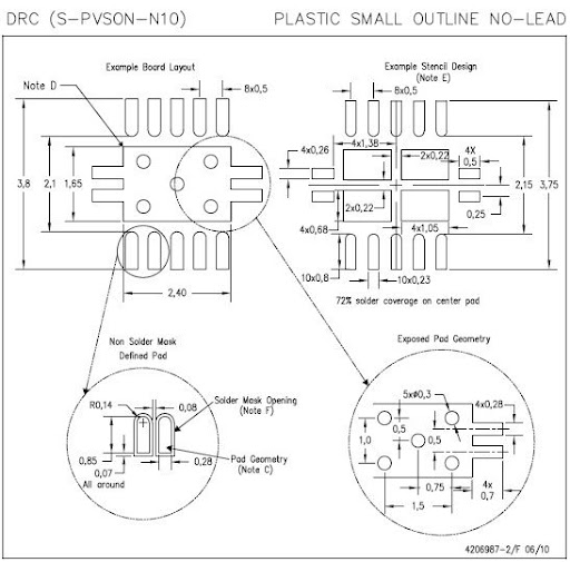
As part of the new design and "new to designing with Cadence" process, I am creating parts for our library and I'm having some trouble with a TI SON part that includes a thermal pad or power pad. Here is a snap shot from the TPS6120:

 TI TPS61202 Footprint

At this point, I've made the pads in the padstack editor (but made them rectangles since I didn't know how to make it a rect at one end and rounded at the other) and used the symbol creation wizard to make a SOIC. To make the thermal pad I placed a filled polygon on the Etch/top layer and it is one large pad with the outline like above.

Question: How do turn my filled polygon into a ground pin (or should I not?) and how do I add the soldermask layer to something I've drawn like this?

Question: How do I add vias to my footprint? My plan was to create the via in the padstack editor then place them in the appropriate places but I have some confusion as to whether the pad/via structure is just supposed to sit there dangling or if it should be assigned a pin # (ground).

I did search the forum and came across the thread Thermal Pad Shape with Vias In it a poster mentions that he makes these pads using multiple surface mount style pins. I think I can figure out how to do this but I'd appreciate any tips on setting up the tools and pads so that things are properly done.

Picture of the pad made from pins:

pad of pins

At Board geometry the AST layer not get enabled?

$
0
0
In the Editor 16.5, at the board geometry----->Assembly Top layer is not get enabled. During the art work generation also the file is be not get enabled. the image is below. So any solution for this option. Thanks & Regards.. Dhamodharan

Generation of NC drill parameter saving?

$
0
0
I had generated the Nc drill parameters for the board. After that i wan to edit the drill symbol size from 0.8mm to 1.00mm, how can i do it. In case after generation of the NC drill parameter file.

Still some unclear able doubts are...

1] I had specified the drill symbol characters from the 1,2,3,4,A,B,C,D,E.But the symbols enabled in the drill chart  is too small in size.

2] In case i generate the NC drill chart means, the output file, where it is saved?

Interlinking Allegro with CAM350

$
0
0

 I am trying to interlinkCAM350 with Allegro PCB editor.

While enabling Cross Probe Allegro in CAM350 its giving message as "start Allegro and the DstCAM350() script. "

can anybody tell me about this script file and the procedure to interlink these tools?

In footprint creation how initialize the default height for the components, in footprint creation option?

$
0
0

Hi..

I had created the sample footprint with the recommended specifications provided. After the creation of footprint, the i had saved it as package. After that specified the component height 0 to 15 mm .Then finishing the i had opened the file in saved folder. In the text document is get enabled. I had opened it, in that package height is not defined. What the mistake i had done during the footprint creation.

Thanks & Regards
Dhamodharan


On OrCAD Signal explorer 16.5 learning basics?

$
0
0
I had finished the pcb design. Then i am trying to learn basics of the signal explorer with OrCAD 16.5. For that i need some tutorial links or any website references or any author basic tutorials. I am having the little bit idea how to use that software. Then before some days i had worked on the simple circuits too. That worked circuits also been get simulated with the low voltage design.Any tutorials or solutions for learning the signal explorer. Thanks & Regards Dhamodharan

Drawing the silkscreen oulines the width of the shape can be increased?

$
0
0

Hi.

I had created the footprint and then i had tried  to put the shape outline for that, i want to increase the shape outline width it is possible from 0.127mm to 0.254mm. Is there any option to increase the width of it.

Thanks & Regards.
Dhamodharan


Layout Plus - connect two separate designs

$
0
0

Dear,

I have already made two PCB layout designs in Orcad Layout Plus 16.2.
I have made PCBs and have tested them.

Now I want to connect the designs, because final design consist of that two boards that I have made before and some other components that I want to add.
Is there a possibility to simply connect/copy/integrate separate layout PCB designs.
That could make me less work routing and placing whole components once more.


BRGDS,
Chris 

Modelling a non-linear load

$
0
0

hi everyone,

i am a very beginner at PSPICE modelling and I would like to get your suggestions on modelling a non-ideal load with Capture. I have a very large set of values for the IV characteristic and I would like to use them in order to build up a new part on SPICE.

Could you help me? 


Thanks a lot

Nicola 


how to split I/O bank in BGA package

$
0
0

hi

in order to swap pin conveniently during pcb layout , i want to split I/O bank in BGA package , just like the attached picture, not manual drawing, is there any simple method  to do this?

allegro16.3


thanks!

PCD Design Process

$
0
0

 Hello,

I'm a newbie in Orcad Layout.
Can anyone help me in understanding the best design flow in PCB layout process.
I suppose that the process is listed in this way for a 2 layer board (top and bottom):


1) Place components;

2) Place outline and other obstacles;

3) Route top and bottom plane;

4) Add copper area on top and bottom planes connected to GND net;

In some tutorial I have found that copper areas are placed all over the board and then the routing is accomplished, but this sounds strange for me.
I'm always afraid by the idea that some vias or IC pads can't be connected because there are too obstacles all around and the power plane can't reach them.
Please let me know what's the bast way to proceed in order to have more possibility to complete the layout without problems.

Best regards.
Lorenzo

After editing the schematic part, the symbols are not get updated in board?

$
0
0
I had placed the component, then for the routing convenient the part pin has been swapped in schematic. After the swapping of pins i had updated the net list option. In that what option should i gave to board option.? In case i m try to update the net list means, net list fails The image is been below. Any solution for the problem occurs.

Symbols not found?

$
0
0

Hi everyone,

So I'm importing my netlist from Orcad Capture to Allegro PCB Editor and when I do Import -> Logic I get 13 warnings that read like: 

#1 WARNING(SPMHNI-192): Device/Symbol check warning detected. [help]WARNING(SPMHNI-194): Symbol 'C0603_SMD' for device 'CAPACITOR NON-POL/SM_0603_C0603' not found in PSMPATH or must be "dbdoctor"ed

Now I've gone to Setup -> User Preferences -> Paths -> Library and set my psmpath and padpath to where the symbols and pads are stored. Is there something else I need to do? 

The rest of my design files are in a different folder than my symbols since my symbol library is large. Is that ok?

When I try to go Place -> Manually and select a part that didn't have an error nothing gets placed on the board either!

What am I missing here? 

Any help would be greatly appreciated!

problem with IGBT model from advanls Lib

$
0
0

Hello,


I am tying to use the AA pspice to tune the IGBT parameters.I am using orcad 16.3.

When adding the IGBT component from the "advanls" library, a simulation error occurd! Although the IGBT is connected and there is no floating pin, I have a floating pin error message:

"ERROR:  [NET0085]

Part Q1 has no 'RCA' property"  

Can you please help.

Hussein 

Viewing all 5525 articles
Browse latest View live


<script src="https://jsc.adskeeper.com/r/s/rssing.com.1596347.js" async> </script>