Quantcast
Channel: Cadence PCB Design Forum
Viewing all 5525 articles
Browse latest View live

Does any conversion capability available for .brd conversion?

$
0
0

Hi.

I  had done projects in the higher version of 16.6 latest hot fix.But my colleague's  PC they using Cadence 16.3. But i want to open files from the higher( 16.6) board  in  lower version (16.3)  of board files is possible or not?

Does any conversion capability software is available on OrCAD market place


Can't update Dynamic Shapes?

$
0
0

I'm stuck in the strangest predicament, and hoping someone can help.

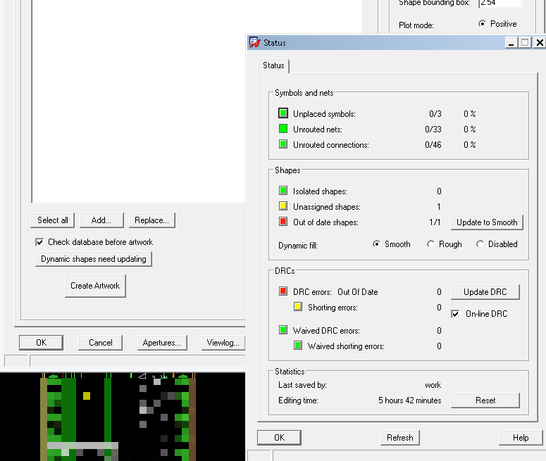
I am ready to create Gerber files for manufacturing, and am met with the "dynamic shapes need updating" error as shown in pic01.

Then I click on the red square next to "out of date shapes" and it gives the location, albeit randomly. If I re-open the gerber dialog and follow the same steps, I get a different location for the problematic shape. See pic02 and pic03 for examples of the shape changing locaitons.

Has anyone seen this behavior? Sometimes the location given for the shape is near 0,0, which I check and can't find. Other times it is located well outside the drawing extents. Is there anything I can do to essentially nuke all the dynamic shapes? I don't need any in this design anyway... I had dabbled with the idea but realized I don't need them.

Thanks a lot for any help,

Jim

Multiple pins on top of each other

Missing all footprints except the first page of schematic

$
0
0

I have multiple sheets of schematic, but when I create the netlist and forward to the PCB Editor, it only shows footprints for the parts on page 1 of the schematic. Anyone knows the solution? I have done a few dozen boards with this version (16.6 S050) and this is the first time it happens.

Thank you.

Silkscreen in Allegro 3D STEP export

$
0
0

Hello,

I've successfully exported STEP 3D models from Allegro and it works very well.  The one thing it seems to be missing is the ability to include silkscreen layers in the export.  Is there any way to do this?

Thank you,

Mike

Set minimum drill hole size

$
0
0

In PCB Editor, how do you set the minimum drill hole size in the Constraint Manager? I'm looking to create various sets of constraints based on PCB manufacturers.

How to include a custom report file like Comp_Place.txt in the Allegro Report menu

$
0
0

Hi,

I am looking for the way to include my custom report file in the Report menu. 

Thanks,

Regards,

TiBo

Snake mode disable

$
0
0

Hi
I'm evaluating 16.6-2015 and am playing with snake mode.  I found that once I select it during a route any further routing that is not dangling won't start routing.  I get an error message in the command window saying that the line must be dangling.

Got it.  Now how do you turn it off without clicking on a dangling route?  The only method I have found is to create a dangle and then RMB->Snake off

Is there a way to kick off snake mode through another menu?

Thanks

Bill


Allegro keeps giving me an error message everytime i try to Place Manually a symbol (6 pin connector con6)...the message says: ""E- (SPMHGE-82): Pin numbers do not match between symbol and component. Run dev_check on device file for more informat

$
0
0

Allegro keeps giving me an error message everytime i try to Place Manually a symbol (con6)...the message says:
""

Placing J1 / CON6_CONN6_CON6 / CONN6 on Top.

Select elements to place using tree view.

E- (SPMHGE-82): Pin numbers do not match between symbol and component. Run dev_check on device file for more information.

""


When I try to place the symbol, I can see the outline of the symbol but it does not let me to place due to the above message.

Please, anybody can help? 

please reply to this post or to my email

fabmaster.out

$
0
0

Hello

fabmaster out is looking for COMP_HEIGHT

Where is this assigned ?


Our vendor is complaining because this field in not populated.

Thanks,

Les

How to import color pallet of an old design to a new one

$
0
0

Hi,

I want to use my previous design color pallets in a new one. I tried to save its file and load it into new design. However, it doesn't work. I can't see colors of my previous design in new design. Is there any other settings that I need to done before loading file?

I appreciate any help.

Hossein

Acid trap

$
0
0

Hi,

Just wonder if there is a skill code for checking Acid trap on copper out there?

Thanks,

Regards,

TiBo

Dynamic Shape is not applying DRC around different net!.

$
0
0

Hi,

I have defined may shape in internal plane as dynamic and have a constraint of 10Mil between various nets. However, My shape seems to connected directly to the via of other net in Figure 1:

If My shape is near a via of different net, then it applies that spacing constraint?!!! Figure 2 shows it:

I have tried Display-> status Update DRC so many times but it doesn't show any Error.


I would appreciate any help.

Hossein

Units of TL length

$
0
0

Hi,

The SigXplorer always displays the length of TL in mils independently of whatever units was it given.

How can it be set to display the length in mm?

Thanks


PCB Factory Design

$
0
0

Hi everyone,

I am wondering if anyone can help me, I want to know (approximately) the area required (by area I mean the size of a room capable of holding all the machines with space to operate them) to manufacture 400 PCBs per day with a average number of components. I can't seem to find this information anywhere so any input would be a real help. 

Also, not as important but if any of you have an idea about how much the machines capable of manufacturing this number of PCBs per day would cost (approximately) that would also be very useful. 

Thank you

Differences between Allegro and Altium Drill format

$
0
0

Hi all,

Our new manufacturer is complaining about our NC Drill file format and  is asking us to give it them in Excellon format or something like Altium Drill file. I am wondering if we  can configure Allegro PCB to give Excellon format or something which is like Altium Drill file. Otherwise they can't start manufacturing. Is there a way to convert these file formats?! Can we configure Allegro to give us its Drill file in Excellon format?!
I would really appreciate any advice,

Hossein

4 layer pcb design

$
0
0

Hi,

I'm new to four layer pcb design. I have designed two layer PCBs using orcad 16.6. So i'm somewhat familiar with orcad tools. But i'm going to design a circuit which includes ECG filter, USB lines, accelerometer etc. So i think its better to use 4 layer board than 2 layer for better performance. The controller used is having BGA package having pin spacing around 0.5mm and diameter of each pin is 0.3mm. I haven't designed a board that includes a microcontroller having BGA package before. Please tell me how to make its footprint and how to route it. I use USB data lines so differential routing must be employed. Please explain more details of differential routing. Also share the steps involved in multi layer pcb design. Any help would be appreciated.(i'm using cadence 16.6 for pcb design)

Regards

Properties attached to drc error RAVEL_MARKER_DESCRIPTION = Soldermask and Board Outline Minimum S pacing on Bottom Layer EXTERNAL_DRC_VALUE = 75.0

$
0
0

Hi,

I have this annoy DRC about soldermask spacing. Could anyone help? I just want to get risk of these. Thanks

LISTING: 1 element(s)< DRC ERROR >

  Class:           DRC ERROR CLASS
  Subclass:        ALL
  Origin xy:       (2320.029 12.700)
  Constraint:      Externally Determined Violation
  Constraint Set:  Soldermask and Board Outline Minimum Spacing on Bottom Layer
  Constraint Type: EXTERNAL REFERENCE

  Constraint value: 75.0
  Actual value:     71.0

  Properties attached to drc error
    RAVEL_MARKER_DESCRIPTION  = Soldermask and Board Outline Minimum S
                                pacing on Bottom Layer
    EXTERNAL_DRC_VALUE  = 75.0

  - - - - - - - - - - - - - - - - - - - -
  Element type:    SYMBOL PIN
  Class:           PIN
  location-xy:  (2256.029 12.700)
  - - - - - - - - - - - - - - - - - - - -
  Element type:    SHAPE
  Class:           BOARD GEOMETRY
  Subclass:        OUTLINE

This is an old style non-associative dimension

$
0
0

Hi all,

In 16.6, when I export a sub drawing with dimensions then import it back into another design I get an error " This is an old style non-associative dimension that cannot be edited this way"  I was wondering if there was a way to make it so it recognizes it as editable dimension?

This is going from 16.6 to 16.6.

Any help would be appreciated.

Viewing all 5525 articles
Browse latest View live


<script src="https://jsc.adskeeper.com/r/s/rssing.com.1596347.js" async> </script>