I have a PCB Antenna reference design in CADSTAR SPL gerber file and I want to copy the PCB antenna to my board design in Allegro. How can I import CADSTAR SPL gerber file to Allegro?
Thanks.
Kevin
I have a PCB Antenna reference design in CADSTAR SPL gerber file and I want to copy the PCB antenna to my board design in Allegro. How can I import CADSTAR SPL gerber file to Allegro?
Thanks.
Kevin
Hi All,
I am making the PCB of SI1143 gesture control. I am making the 2 layer PCB , (Top & Bottom). I have three connections along with other connections.
I have a confusion that how can I represent the connection of VCC and ground.
I am giving two voltages to my circuit and one ground . Since in Schematic, I connected the circuit with symbols like VCC and ground. But in PCB editor how can show the connection of VCC and ground ?
How to make the connection of Vcc and ground by Via in PCB editor.
Can somebody suggest me for this as soon as possible? I am stuck at this point.
Dears
I am new to the tool, and I am being blind with this new assignment.
1. I want to design a 4 layer board (RF for 50e imp matching on three tracks: basically a SMA input).
2. We will be using a rogers material (RO4000) with the thickness given as 10 mils(0.254mm).
3. metal01>>rogers core>>metal02>>prepeg>>metal03>>fr4 core>>metal04.
4.total thickness of the board0.062in/1.6mm with 1oz of cu on top and bottom metal and 1/2 oz inner metals.
5. How to setup for design, stack up design and values. Your precious advice need and appreciated.
Am already working on the design and am half way stuck after netlist generation.
Hi All,
I am making the PCB of APDS-9960. After completing the process of Artwork . I went for Silk screen. I chose
Component Value: None
Device Type : None
Board Geometry: Silk
Package Geometry: Silk
Reference Designator: Silk
Tolerance: None
User Part No: None
Minimum Line length: 8.00
Element to pad clearance: 5
then click on silk screen and saw that except that IC Reference designator there is no reference designator of other elements. And the same time there is no board outline. I don't why was this happening.
Can Somebody suggest me for this ?
Thanks in Advance
Good day every one!
i use Allegro CIS & PCB 16.6
I have complex hierarchical design divided into several pages. Each pages included couple of several logically separate circuits. I want to move some of those circuits to another page for better readability of the whole schematic document.
Copy - delete - paste to another page should solve the problem BUT the problem is that I already have routed design. And any refdes changes from CIS after creating netlist and update brd file caused moving connetions and etch removing.
Actually parts are not moving - it moving connections from them - see picture.
For example i rename two parts in schematic R3 -> R4 . Then Tools -> Create netlist (with option of update board file) -> after netrev it open brd file and see that refdes of the part dint change their old places , so all old clines will be lost.
Options->Preferences->Miscellaneous->Preserve reference on copy did not help, maybe because i have more than one hierarchical blocks in schematic/
See pictures with changes and settings below
So my goal is to change refdes`s of components from schematic WITHOUT ANY changes of routing in brd - how i can do that ?


anyone knows when designing pcb ,how to transform BRD file to EAGLE file?
Is there a way in Capture CIS to set default properties for new schematic symbols? For example when I create a new part I want it to include the following properties with blank values:
- Manufacturer
- Part Number
- Description
- Link
I have read other posts about people copying and pasting components that already have these properties associated with them, but that is just a work-around, and not a solution. That also won't work when you create a new part from a spreadsheet.
Using Orcad PCB Designer 16.6
When routing a board, I keep finding that several traces become disconnected from the pins they are routed to. It looks like the trace connects to each pin, the trace and pins both have the same net and are on the same layer, but a ratsnest is shown and the trace does not move if the symbol is moved.
This is an ongoing thing. Just when I think I'm done routing, I check the design status and there are hundreds more disconnected nets. Sure enough, traces that have already been routed have become disconnected.
I had a theory that this may be related to using place replicate, but it now seems to be happening to traces that are not associated with a place replicate group.
Does anybody know why this is happening and how to stop it?
Hi,
I'm using a controller having LFBGA package having pitch 0.5mm as shown in the attached image.
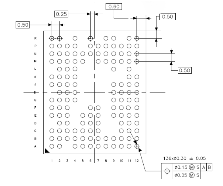
I've designed the footprint for the controller. Land dia is 0.24mm. My board is having six layers and i have used several vias for taking connection out of the controller. The vias i used were 0.15mm drill dia and 0.30mm regular pad. When i sent the gerber file to PCB fab house, they asked for some correction since their minimum IAR/OAR is 0.125mm. They found minimum OAR/IAR around 0.025mm for the drills of 0.15mm end dia. Their formula to calculate annular ring is as follows :
OAR / IAR = (Copper pad diameter - TOOLSIZE)/2
TOOLSIZE = ENDSIZE + 0.15mm for all PTH holes
+ 0.05mm for all NPTH holes
My question is how can i correct m design according to their requirement ? I have to choose copper pad dia of 0.55mm(for a drill of 0.15mm) to meet their standards. But since its a tight layout using .55mm vias will be practically impossible(pad to conductor spacing recommended by the fab house is 0.127mm). How can i complete my design from this challenges?
Any help would be appreciated.....
Hi
In creating library part, if i change the Setup - -> Design Parameter - - > Design, the width and Height not able to modify,
It is showing the following error.
can't reduce upper y extent
Please help to resolve this issue
Regards
Prem
Have you had Overseas Trading Experiences and have you ever buy pcbs from china ? if you did,how do you think so? satisfied? disappointed??
and about the quality,the service ,and the shipping time and so on , come on here to discuss and communicate together. and give some views about chinese PCB manufacturers, many thanks.
Dears
Can you please help to understand the different GND via stitching for my recent RFboard.
1. Along the 50E imp track.
2. Below the IC thermal pads, is it at component level?
3. Also via scattered through out the board.
I have followed the path ( Place>> Via array>>Boundary and Matrix) but unable to get the desired result and uniformity.
Many Thanks
When exporting pick and place data from OrCAD PCB Designer, how is the body center calculated? Is this related to the pins, place_bound_top, or something else?
Hi all, I am designing a 6-layer PCB in which I need to place 'L' shaped cutouts. I have tried making them as internal board outlines which means it gets included in the board outline part of my Gerber file. However, my pcb manufacturer wants any cutouts to be in the drill layer. Is there any way I can get the cutouts in the drill layer? Note: I used the method shown in the following video tutorial: 
Hi All,
I was making the 2 layer PCB of Gesture Control.
- I went to generate my artwork only to find out I can't because there is a database error.
- I check dbdoctor.log and it says "Error in Attribute Pointer to Void Invalid", 1 error could be fixed
- I do a database check (including regenerating DRC errors) and it reports that 2 errors were fixed, both referencing the same error message above.
- Sounds like I should be good to go, but when I try to generate the artwork again, I get the same error message and the cycle continues.
Can somebody suggest me how to resolve this Problem?
Thanks in Advance
Share a Chinese PCB manufacturer to you who need pcbs ,PCBGOGO is a Custom PCB Prototype Manufacturer in china, With rich experience in PCB fabrication and assembly, high quality, low price, fast lead time, and quick response are their advantages..
the best part is their Instant online quote. and detailed tracking system ,so that you will know where your money is going when you have ordered and will inform you the each process of the PCB boards after you pay. You can enter www.pcbgogo.com/f to know more about them, sincerely hope to help you that in need
I'm using Allegro DE HDL in conjunction with a part table file and I can't quite wrap my head around how the two mentioned properties work together. I think that JEDEC_TYPE is meant to point to the actual footprint (.psm file) that you want the packager to use. But I don't understand how PACK_TYPE is meant to be used.
Any help would be appreciated.
I setup a number of matched length groups and now I get the message "Field solution failed" during routing. How do I disable this from occurring ?
Hi experts,
I'm working on board, which has a GND structure like below. While I found even the symbol name is different (GND_A, GND_B), while the net name is all "0". Can you tell me how to solve this problem?
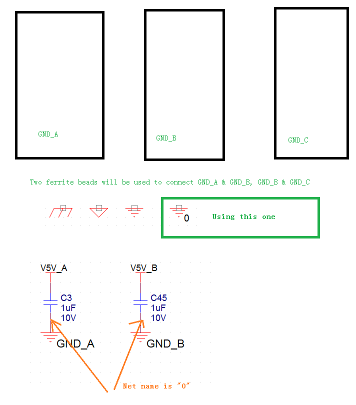
Thanks
Chris
Hi.
Which mouse and keyboard combination do you preffer for working with EDA design?
/Matias