Quantcast
Channel: Cadence PCB Design Forum
Viewing all 5525 articles
Browse latest View live

Create solid thermal vias using Orcad

$
0
0

Hello,

I need to create a solid thermal via to be used under a powerpad package. The specification of the via is mentioned below:

1) The thermal vias should make their connection to the internal ground plane with a complete connection around the entire circumference of the plated through hole. Place a ring of exposed copper (0.05 mm wide) around the vias at the bottom copper plane.
2) Do not cover the vias with solder mask.
3) Do not use a thermal relief web or spoke connection.
4) The recommended via diameter is 0.3 mm or less.


Could someone help me in creating such a via using Orcad? Should the via be created while making the footprint or during the layout?

Thanks.

Ananya

Multi-level backups?

$
0
0

Okay, so I went and got my Schematic corrupted beyond recognition by an unfortunate part replace option. Also the backup save (DBK) picked up the changes. Now fortunately I only lost about an hour's worth of work as I had changed project name not long before.

However, Capture claims it's got multi-level auto-backup feature. This does not actually seem to work or I'm missing something? I've got it set to 10 minutes, 3 levels, directory . 

OrCAD Capture TCL to Iterate over all pins of a part in a Library File

$
0
0

Hi All,

I am new to TCL scripting in OrCAD Capture and wanting to write a simple script to

iterate over all pins of a part (multiple sections) in a Library file, and to print each of the pin number.

I have got an example from the user guide, to iterate over all pins of a part instance/ drawn instance:


set lIter [$lInst NewPinsIter $lStatus]

set lNullObj NULL

#get the first pin of the part

set lPin [$lIter NextPin $lStatus]

while {$lPin !=$lNullObj } {

#placeholder: do your processing on $lPin

#get the next pin of the part

set lPin [$lIter NextPin $lStatus]

}

delete_DboPartInstPinsIter $lIter

Just wondering how i shall proceed from here...

e.g  the Library file is "my_Library.olb",

the name of the part is "Our_Chip" and it comes with multiple sections.

Appreciate if any TCL expert can help, Thanks in Advance.

Capacitance Measurement - Via

$
0
0

Is there a way to measure the capacitance between two vias in Allegro on a given layer?  Is there a product Option I need?

Thanks,

Wild

Unable to use tcom package for Active Tcl 8.6 in cadence 17.2 version.

$
0
0

Hi

The tool OrCAD is not able to recognize the tcom package used by Active Tcl. We are using this in the 16.6 version which uses Active Tcl 8.4 however.

At the command window, when I invoke "package require tcom" the following message is returned

Capture> package require tcom
[ 1]couldn't load library "C:/Cadence/SPB_17.2/tools/lib/tcl8.6/tcom/tcom.dll": invalid argument

But the tcom package contents are present at this location.

Does it have anything to do with 32 bit version of Active Tcl 8.6 ? What is the version of Active Tcl that comes default with 17.2 version. i would like to understand the flow

Thanks

No DRC error when placing or sliding vias over inner traces

$
0
0

Hello, I have been having the weirdest issue lately.  I am working on a 6 layer board with 3 routing layers.  I have a routing layer at the top, a inner layer, and a bottom routing layer.  Currently, when I place a via it will let me place it right on top of on of the inner traces with no DRC.  I first noticed the issue when I randomly spotted a via going thru an inner trace.  I tried to slide the via away and expected the inner trace to 'bubble' around it like normal but it didn't.  I tried to place a new via and it allowed me to do the same thing.  One interesting thing is that if I slide the via right on top of an inner trace, exit the slide command, then initiate the slide again, it bubbles that inner trace out of the way, but if I drag that same via over near any of the other inner traces it acts as if they aren't even there and will let me place the via right on top of them again.  Also, if I go to 'slide' an existing via that is going from top>bottom then back to the top again it will let me place that via on an inner trace and the same issue repeats; however if I 'slide' a via that goes from top>inner or bottom>inner it will 'bubble' the inner traces out of the way like normal.  To my knowledge all of my constraints are set correctly, on-line DRC is on, and none of these are blind/ buried vias.  I have also ran DB doctor but it found no errors.  This is the 4th revision of this board and it has not been an issue at all before this point.  I was able to go back and forth between older revisions of this same board and the 'slide' function was bubbling the inner traces away as it should on the older versions.  Placing a new via right on top of an inner trace caused a DRC error properly as well, but when I returned to my current revision it was still not working properly.  However, for some reason a day later now all of my previous revisions of this board are exhibiting the same behavior.   I am really hoping this is something super simple because this issue has caused a lot of delays on my end.  Any help would be greatly appreciated.  

I am running version 16.6 SO60

Auto create report vs statistics for checking unrouted nets

$
0
0

Hello,

I am using orcad layout. To check the unrouted nets, if i use Auto-> create reports and select 'Conn unrouted', it shows no unconnected nets. However, if i check the 'statistics'  spreadsheet, under routing statistics, it shows 86% routed.


I am not sure which one to believe. I don't see any ratsnest when all the nets are enabled for routing. Also, the statistics spreadsheet doesn't show which nets are unrouted.

Please help me out.

Thanks.

asenapati

Extract coordinates for pins in design.

$
0
0

I need a way to get an extraction/report of coordinates for pins of the connectors in the design.
I am designing a test fixture, and need the coordinates for test pin location.

How do I do this?

Br,
Martin


How to define the rotation by single step value?

$
0
0

Hi.

I want to  rotate  the componet by incremetal values of 1,2,3,4,5,... etc in degree incremental values. So i had to tried incremental values. But the component can't able to rotate the manual values entered by us. 

Then while doing the rotation default angles are be get rotated. Then i had tried to change the values in pcb env env. editor too.

While opening the editor the line getting error message.

Curve option in Route>Slide disappeared in 16.6

$
0
0

Hi,

I am new to 16.6 version.

In 16.5 or older versions there were an option in Route>Slide that we can change a 45 degree routed net to curved routed net on clicking.

But when I used slide option in 16.6, there is no curve option. there is an option here named "Vertex Action". In the Vertex Action drop down window there is an option of "arc corner" but it is not working.

Regards

Tanveer

ratsnest by class

$
0
0

Hi <

IS there any way to select a class of nets and then have the ratsnest displayed ?

Plot only selected parts in design.

$
0
0

Hi,

Is there a way to sort the parts/symbols that I want to see or plot to file?

I want a plot where I can see only Test Points, and not the other parts in same layer.
My test points are SMD in bottom layer.

Thanks,

Martin.

OrCAD Capture Tcl script to change page names

$
0
0

Is there a way to change the name of a schematic page in a Tcl script?  I'm able to use code similar to the example in the Tcl/Tk Extensions manual to print out all the schematic page names, but I can't seem to change them.  The log in the command window shows calling the Menu "Design::Rename" command, but I'm looking for a way to rename pages without opening up dialog boxes.

LQFP-80 Small to Standard

$
0
0

I made a mistake on my PCB. One of the footprints on my PCB is supposed to be the small LQFP-80 (.4mm pitch), but I had the board printed with the regular .5mm pitch LQFP-80. I've trying to find some kind of socket adaptor of something to workaround the problem. I haven't found anything yet. Does anyone have any ideas? Or should I just give up and order another board?

How should change capture.ini to link my CIP database?

$
0
0

I have CIP databased installed on a separated server with known IP address and machine name. After install CIP client in my Win10 working station I am requested to modify my capture.ini to change its "Configuration File"'s content to lead to this database. What is the proper format for it? Since it is not on local machine, but on a server with IP, I use 

Configuration File = \\MyServerName\CIP-E\Configuration_Files\CIP-E V6.0 CIS DB.DBC

But the tool claims that it can't find it. What is the proper format for this file path?


How to update a footprint within "Part Developer"?

$
0
0

Hi!

I created a part in Part Developer, the footprint in PCB Editor and associated it by selecting a Jedec_Type within Part Developer, the footprint got associated but I recently made some changes on the footprint like adding some silkscreen info.  
Does anyone know how to update/refresh the footprint within "Part Developer" and see it reflected in the Package's associated footprint?

Not sure if this is the correct flow so I'm open to suggestions.

Regards

-Jose. 

Should CIP web server and CIP database on a single machine or separated machine?

$
0
0

We have CIP 17.2.011 web server and database server separately installed on two virtual machine. I need to update datasheet links with its real location (on DB server's C:\Cadence\CIP-E\Technical_Datasheets). The question is:

1. Should I run Rapther from web server or database server (they are on different virtual machine)?

2. What new path I should use? I put //MyDataBaseServer/Technical_Datasheets with http:// start, but it seems dosn't work. 

Any suggestions?

CIP license error

$
0
0

We have CIP installed with one license only. We found that once a user access to CIP database and exit, other users can't access CIP any more even no others login. The following error messages appease on the page:

--------------

License Error.

Unable to obtain license.

Message: CIP license checkout failed.ERROR (LMF-03004): License call failed for feature orcad_component_portal, version 17.200 and quantity 1. The license server search path is defined as 5280@CYPRESS-WEB;5280@localhost. The FLEXnet error message is as follows, FLEXnet ERROR(-4, 0, 0): Licensed number of users already reached. Run 'lic_error LMF-03004' for more information.

----------------------

The strange is: the first user is still able to access and exit without problem. How we can check who is occupy the license?

Creating Schematic Symbol With Smaller Grid

$
0
0

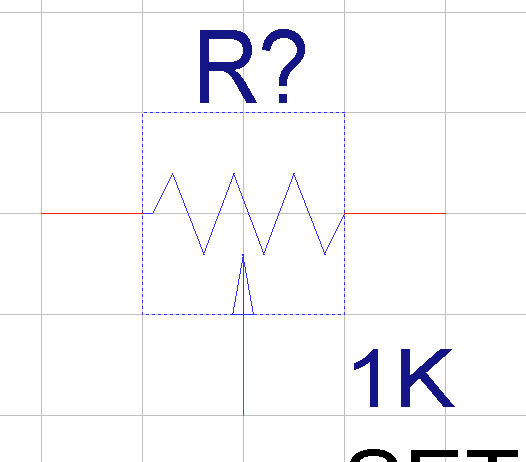
I'm sure I am missing a simple setting but after spending too much time looking for it I figured I'd come here. I want to have a smaller grid for component creation than for schematic creation, so I can create symbols in finer detail. For instance, below is a photo of the stock potentiometer, which clearly has lines that are not docked to the regular grid (1-1 pin spacing). However when I try to replicate it my lines snap to the grid. Any help would be appreciated.

Diff Pair Nets are displaying errors when necked down

$
0
0

We are using a diff pair with the default gap at 15thou and 15thou width, but we also have the necked trace and gap set at 6thou.

When routing, the 15th is fine but when we route to a fine pitch IC and attempt to neck down the traces, we get a width and spacing error appear. It is as if the necked traces are not working.

Any suggestions? We are running 16.6.

Viewing all 5525 articles
Browse latest View live


<script src="https://jsc.adskeeper.com/r/s/rssing.com.1596347.js" async> </script>