I am trying to reuse a previous layout by using a module. When I pick 10 components, I can place the reuse module on the new design without issue. When I try to fully populate (over 500 components), I am consistently getting a "Text Line Outside Extent" issue and the 3-4 hours of work in associating components just simply disappears. This has happened 3 times in a row. Is there a limit on how many components a module can associate ? Is there a preexisting location that I need to set before associating components ? Is there something else that I am missing ?
↧
Text Line Outside Extent and reuse module
↧
Creating complex shapes and importing them from .DXF ino pad shapes...
Sometimes I have to create complex pads for footprints (like the small AVX 9175 wire to board connectors).
In such cases, AutoCAD is my best friend. It handles "lines and stuff" in an excellent way and it is easy to create
complex shapes and "polyline them" which then can be easily imported into the Cadence PCB Editor environment
and then into the Padstack Editor. Also using drawings from connector manufacturers by extracting the
top view in an appropriate scale and then importing them as incremental and mapping the imported
.DXF layer to geometry/outline (or silk) saves hours of tedious work.
But:
Why does not Cadence PCB Editor honors the coordinate and origin settings in the imported .DXF?
I do set the 0,0 in the center of the shape .DXF. I do limit the extent of the .DXF to be just covering
the outlines of the polyline shape in AutoCAD before saving the .DXF for later Cadence Import.
When importing a .DXF polyline shape, the PCB Editor seems to randomly choose origin 0,0
and also the extents of the imported shape. When importing a complex figure such as a flat cable
connector outline or even an ordinary thing such as a large DSUB connector outline, all of a sudden
the extent of the editor canvas is enlarged and the imported .DXF ends up far away from the
"copper" or other parts of the footprint-in-creation.
This behavior is present in 17.20 as it was in 16.6
Has anyone else experienced this? Is there any way to correct it?
↧
↧
Allegro Design Entry HDL 16.6 Hierarchy - How does it work
I have used hierarchy designs before using OrCAD Capture and it was easy and intuitive to use.
But how do you use hierarchy designs using Design Entry HDL? I have a few designs with the top level set, I add blocks to my top level and I get errors saying there are ports not available in the lower sheets. But how do I add these? How are nets named across sheets? How are additional ports added to both lower and upper level pages and blocks? How is the multi-sheet environment controlled to maintain the part idents seperate? I have one sub-level with 3 sheets and another with 2 sheets, but the page numbers go 1/3, 1/3, 2/3, 3/3, 1/2, 2/2??? there are 6 sheets (including the top level) the hierarchy shows the pages as 1, 2, 3, 4, 5, 6 but the actual page borders are nothing like the correct order or quantity.
↧
Hide bias voltages
Hello,
I have a schematic that I started as a hierarchical design, ran some simulations, and then changed re-annotated all my hierarchical designs so I could produce a PCB.
(I think) that since this broke the link to my simulation results, the entire spice toolbar is greyed-out. That's ok - I don't need the simulation anymore. But all my bias voltages are still visible, and it seems I can't hide them by clicking on the big green V anymore (since it is greyed out and non-responsive). They obscure component values and generally what's going on in the circuit. I can delete/move them manually/individually, but there are a lot of them. Can I somehow hide them all en-mass?
Thanks!
↧
ERC Error: "Output Connected to Bidirectional Port"
Hi,
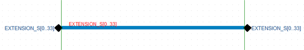
I am making a hierarchical top-down design in Design Entry CIS v16.6. The root schematic has hierarchical blocks connected by Named Netgroups; the hierarchical pins have been designated as "Bidirectional" with the corresponding Netgroup associated with it. (An indicative image included below)
On descending the hierarchy, the schematic has both inputs and outputs from ICs connecting to the Netgroup port .
When running the DRC, I get the "Output connected to bidirectional port" error. Since the ports actually represent Netgroups (with inputs and outputs) I was not expecting this kind of error. Am I missing something? Any assistance in this regard will be greatly appreciated.
↧
↧
HOW TO ADD VOID TEXT IN COPPER POUR
IM IMPORTED A LOGO. It should be placed on top copper pour. but logo text not containe copper (void).
INVERTED TEXT CREATION.
↧
CIS Variant - Cannot Link Database part -
Hi,
I have to build different variants from my schematic and try to link a part in the part manager, that have the same footprint, but a different name for the schematic part.
If I try this I get the message "Cannot link database part on this variant because the schematic parts differ".
My problem is, that I have a pci express connector with different moduls which are connected.
↧
Change shape fill type
Using PDB designer 16.6.
I'd like to put a shape on the silkscreen layer that is a copy of a route keepout shape but is crosshatched. If use the shape copy feature (Z-copy) I can create the shape but it comes in as static solid. I have not found a way to make it crosshatched. I can draw a new on but it's complicated enough that it would be painful.
Thanks!
Yanko
↧
How to re-use old footprints from an Allegro design
Hi,
Simple question (maybe). I have exported the library of components from an Allegro 16.2 layout into a directory. Everything looks perfect. However, and this might be my inexperience, every component, including the surface mount parts, still retain the number of layers that was used in the old layout. How do I re-use those components in a new design that will not only have a different number of layers, but different layer names and functions?
Thanks!
Chris
↧
↧
Manufacturing option menu in OrCAD
How to get the panel editor, dfm checker, doc editor menus in legacy OrCAD menus?
I get those in Allegro PCB Designer and new OrCAD menu structure from Manufacture menu but not in legacy OrCAD?
↧
Board Simulation Issue - Via Model not found
This an FYI for folks doing SI work.
My wonderful IT team upgraded all our PC's to windows 10. At that time they change all user names from first intial last name to fistname.lastname cuasing a major headache for my simulation. When I ran a probe of a signal I would get an error message: VIA Model not found. After hours with the India support team and the Canadain team figured it out: The change in my user name changed the path of my temp environmental path, it now had a "." in the path.
We resolved the issue by changing the Path variable to C:\TEMP.
So beware the IT folks, for they do not understand all issues.
↧
Lock Traces in Layout 17.2
I am trying to route traces as shields. Whenever I duplicate a connection, a trace on another layer, which I inted to be there, but which is a duplicate gets deleted. Is there a way I can lock traces and prevent it being deleted?
↧
Importing OrCAD Capture 16.6 into Capture 16.2 using EDF Importation
Hi,
Thought I had a solution, but NO! Friend has OrCAD 16.6 Capture and has a fairly hierachial schematic. So I had him export to an EDF format which worked fine. However, when I got it, I could import the EDF Capture file, but lost all of the reference designation information. I DID get ref des info, but it appears to have have started at number "1" on each page and there are 45 pages!! Needless to say, this causes a severe problem if I am to synchronize the 16.6 Allegro using 16.2 Allegro for corrections. Right now, due to the schematic have all kinds of DRC errors with duplicate references, etc. I am stuck.
Any ideas out there? Or is this a "bridge to far" going between OrCAD 16.6 to OrCAD 16.2 via the EDF translator?
Chris
↧
↧
3D Step file creation in Allegro?
Is there a way to create a 3D part step file in Allegro during a part creation?
If relying on other software tools is required then when will this feature be incorporated?
Thank you-
↧
Allegro 17.2 Orcad Translator?
Hello. We were just recently upgraded to Allegro 17.2 from 16.6. We have a lot of boards that were done in Orcad 9 and with 16.6 we were able to use the Orcad translator to bring these old designs into the new software. I cannot seem to find that translator with the update. Has it been removed? Is there another option now for bringing .max files into the new software?
↧
Site setting for Drill Chart sizes .DLT
Hi,
I can go into the installation directory and edit the .DLT files to change the drill chart dimensions. Is there a user preference path that can be used to automatically select site generated .DLT files?
This is where the dialog looks: %CDSROOT%\share\pcb\text\nclegend
This is where I want the dialog to look: %CDS_SITE%\pcb\text\nclegend
Thx,
Aric
↧
NCroute file doesn't lineup properly with artwork and drl files
Hi,
I tried to generate the ncroute in the manufacturing to get the details of the rectangular slots in my board design. Unfortunately when viewed in the gerber viewer it was not matching the excellon format and rectified it later though the ncroute files doesn't lineup properly with the artwork as well as the drl file.
Please give any alternate suggestions to make sure it doesn't go mismatch with the artwork.
Regards,
Mukilan P
↧
↧
disabling annotate/back annotate constraints from capture to/from Allegro
I have a schematic with no constraints set. I swapped some pins in Allegro and back annotated the pcb file to capture. This added the constraints from the pcb file to the schematic. If I update the constraints in the pcb file and then load a new netlist the older constraints are loaded into the pcb. Is there a way to load a new netlist without loading the constraints ?
↧
Combine ground nets
I have a schematic with two ground signals - GND_SIGNAL and GND_POWER. I want to combine their netnames so they tie to the same inner plane. Can this be done, and if so, how?
↧
ODB++ file extract error on pin data format during manufacturing
Hi,
I tried to create the odb++ file for the pcb vendor to extract the pin data and to do the fabrication process, he came back saying an error that the pin data on the components in step folder, saying that on top and bottom few data are missing.
Regards,
Mukil
↧