Quantcast
Channel: Cadence PCB Design Forum
Viewing all 5525 articles
Browse latest View live

Transferring user defined property values between Capture and Allegro PCB Editor

$
0
0

If I would like to transfer, say, the component value between Capture and Allegro this is no problem, on the package .dra file I just add a text "*" using the "Component Value" class to some reasonable layer (Component Value -> Silk Top). From the Class dropdown menu it appears that I can also grab certain other property names, like "Tolerance" or "User Part Number".

Is it possible to transfer arbitrary properties between the schematic and layout, or only these ones? In this example I have a 10 position rotary switch. Ideally I would define properties called "position1", "position2" etc. in the schematic library, give them appropriate string labels in the schematic design, and then have those labels automatically transferred to some silk layer in Allegro. Currently I just have dummy text as package geometry > silk top, and then I edit the text manually whenever I place a switch... but this has the possibility of transcription errors.

Thanks!


Orcad PCB design - Status bar shows "cancel?" in a yellow box for no reason

$
0
0

Hello,

I'm using the Orcad PCB design software.  i'm Currently doing the E-training course to be able to use the software.

I'm using the design given with the training manual. After doing a simple "Align the component" command,  the status bar show a yellow box with "cancel?" written inside.

Sometimes after some other similar command,  the software crashes, and I have to reboot it.

I would like to know why does the software keep telling me this "cancel?" thing. I fell like it's the reaon why the software crashes and I want to fix it.  I know this yellow box is supposed to mean that the system is working,  but on what??

I'm using Orcad PCB editor 17.2 on a 64 bits windows 10

Thanks.

17.2 alias shortcuts not working

$
0
0

I'm trying to use the same alias shortcuts that I was using in 16.6 and a few aren't working. 

I had  ~z (ctrl + z) assigned to "rotate", but now it seems to be stuck as "cancel". I'm sure of the env file that I'm using because I can change other things and see the effect. 

I don't like right-click. I'd prefer a single key to do this. Not a function key. I'm using those to change my grid setting.
Any ideas? 

E-learning course for Floor Planning

$
0
0

I am going through the E-learning course for Allegro PCB Editor. In the floor planning lab I am being asked to open this command

the statement reads "Choose Outline-Room from the top menu."

I cannot find this command anywhere. Can someone direct me to where I can locate this.

Thanks much

Capture CIS Lite 17.2 issue: "ERROR(ORCIS-6016)" on save

$
0
0

Today, I installed  Orcad Lite 17.2 on my Windows 10 notebook for the first time.

When I launch OrCAD Capture CIS - Lite (version 17.2-2016) and create a new project, I can not save it  (although it's an emtpy project). Instead I get a strange error message.

These are the exact steps to reproduce this issue:

- Launch Capture CIS Lite

- New Project  - PSpice Analog or Mixed A/D

- Create PSpice Project - blank project

- Save

Then I get the following error window:

"ERROR(ORCIS-6016): Data Source BenchAccess172D not found. The selected part management configuration requires this data source name.

To create the data source or change the data source name, go to the Control Panel and click the ODBC icon."


Has anyone else seen this error? Please advise!

I only wanted to walk through the tutorial available here but I can not even save an empty project. My installation seems broken although I installed OrCAD lite for the first time. Is it because I'm not running the program with administrator privileges? I don't think so. The days where programs had to be run as administrator to work are long gone, right?

Thanks

Dan

Title jumps in schematic titleblock when opened on another computer

$
0
0

Hi, 

When using OrCAD Capture, the title is aligned in the titleblock using the <Title> property. Our .DSN and .opj are shared and controlled using version control software. When another user opens the project, some of the titleblock properties jump around the page and are no longer aligned properly in the titleblock, and need to be moved manually.

Does anyone have any idea why this might be happening and how to remedy the situation?

Thanks
jeff

No dialog box results after clicking Auto > Design Reuse In OrCAD Layout 16.0.0

$
0
0

Greetings,

  After creating a small layout for the purpose of experimenting with design reuse, then clicking Auto > Design Reuse from the main menu bar, nothing happens. I've tried this on one machine running XP SP2, & two others running Windows-7. Layout works on all three. I'm assuming I'm doing it wrong, but haven't found clear documentation for Layout 16.0. What should be happening?

  On a related note, after clicking on Tools > Annotate in the project window of the source Capture schematic, then choosing the Layout Reuse tab, the box "Select schematics to mark for reuse" is empty.

  Where am I going wrong?

  Thanks,

    Steve Kleiser

Allegro PCB Editor

$
0
0

Hi All,  

Is there any solution to find Cline width escape that is greater than the component pad in allegro pcb editor.

Thanks in advance. 


Configuring CIS with MS Access using ODBC mapped to Unix (UNC) Disks in Windows 10...

$
0
0

I have an issue with Windows 10 and ODBC...

It seems that Microsoft has disabled the possibility to map the ODBC driver configuration to an Access database residing on a UNC mapped disk.

We have a Solaris system with SAMBA software that maintains our group areas. According to IT service dept, this set-up is the only one that facilitates a flexible way to set disk quotas and rights in our organization. Previous Windows 7-installation had not have any problems with the CIS database on a UNC-mapped drive, but Windows 10 is a different story. The ODBC canvas refuses to see a network drive that uses UNC. It is not possible to browse for it. It is not possible to map it using text entry. Allegro has no problem finding footprints, and Capture can find the schematic library. CIS does not work.

I am not the only one that has discovered this, and there seem to be a circumvention by editing the registry (Regedit.exe) and define the paths/disk from there, but I have not found any information that is directly applicable to MS Access, .MDB and Capture CIS configuration.

My choice to use Access was based on that it is included in Microsoft Office and that it was adequately convenient to use it as a front end tool when adding part entries. I could consider changing to some other database system, but then the library needs to be converted...

I have logged a support case with Cadence and also with our IT support. In the mean time, my thread is both a comment and a question if others have seen this, or if anyone here has information how to resolve the issue.

Placing a .JPG image into OrCAD Capture 17.2 - what restrictions?

$
0
0

I created a block diagram of my design in Microsoft Visio. This diagram is an 11" x 17" B-size page.  I am trying to place a JPG image of that block diagram into a page of my schematic but there seems to be some restriction that I cannot find.  

At first I thought it was a file size limit of 100KB, but found that not to be the case.  Then I tried creating the JPG with various percentages of quality, from 100% down to 45%, seemingly with no effect.  I've tried various pixel dimensions, from 120 X 120 pixels down to 90 x 90 pixels per inch, and find that I can usually import files with lower pixel resolution, though it takes most of 60 seconds to do so.

So where is it documented what kind of JPG files OrCAD can actually import?  This is kind of important to what my company is asking of me.

For that matter, I've also tried various .TIFF and .PNG file settings when saving my block diagram from Visio and have similar results (i.e. no results... the files won't import)

2 Pads having the same Pin number

$
0
0

Hello

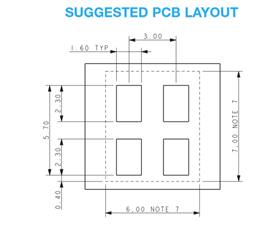
I designed a foot print for a connector" The suggested footprint looks like the one below.  This connecteur only have 2 positions, so this means 2 pads are electrically connected.


on my layout on Orcad PCB editor, i designed one as being the electrical pin and the other one being the mechanical one. The idea is that when I connect the line, i can start from one or the other pad, and the software will know the pin is connected. unfortunately, I cannot connect a mechanical pad, and i cannot design a pad with 2 shapes.

how am I supposed to do it?

Thanks a lot

Allegro16.2 components placing issue

Custom Layer Views Changed from 16.6?

$
0
0

In 16.6 I had a bunch of custom views defined under scripts that I could jump through, bottom view, topview, inner1view, etc.  The change to 17.2 broke all these scripts and it appears the menus have changed internally

16.6:

"cvf layer_tree_item 'Stack-Up'
cvf layers_visible stack-up stack-up/top TRUE
cvf layers_visible stack-up stack-up/soldermask_top TRUE
cvf layers_visible stack-up stack-up/pastemask_top TRUE
cvf layers_visible stack-up stack-up/through_all TRUE
cvf layers_visible stack-up stack-up/package_top TRUE"

17.2:

"QtSignal CVDLayerContainer CVDVisibilityOff clicked
QtSignal CVDLayerTable VertHeader clickedCheckBox 0
QtSignal CVDLayerSplitter CVDLayerTable dataChanged Top Pin
QtSignal CVDLayerTable VertHeader clickedCheckBox 4
QtSignal CVDLayerSplitter CVDLayerTable dataChanged Soldermask_Top Pin
QtSignal CVDLayerTable VertHeader clickedCheckBox 6
QtSignal CVDLayerSplitter CVDLayerTable dataChanged Pastemask_Top Pin
QtSignal CVDLayerTable VertHeader clickedCheckBox 8
QtSignal CVDLayerSplitter CVDLayerTable dataChanged Filmmasktop Pin
QtSignal CVDLayerTable VertHeader clickedCheckBox 10"

Besides not having an easily human repeatable format if I end up having extra layers added the checkbox number moves.  For example, if one design has a MECH layer added to PkgGeo and another has MECH1 and MECH2, that means the scripts will not work the same.  I ran into this on a design where for some reason the placebound bottom was erroneously showing in my topview in one design but not the other. Also one designer took my hotkeys and scripts and he didn't have any inner layers defined and when calling anything that modified etch the editor would crash immediately without a warning.

Is there a better way to view scripts that can transfer through designs?

Deciphering ALG ascii file for Altium footprint import

$
0
0

My question is one of deciphering the Allegro ALG ascii file used for board outputs. 

We are importing footprints into Altium which requires an ascii export from allegro using extracta. I'm able to do that okay, but Altium handles padstacks differently and we lose custom pads on our paste layer (offset and size are different from top). This information is in the ALG file, but I'm told Altium ignores that layer on the import since the mask/paste are defined automatically by Altium.

What I need to do is move the lines in the alg file containing pastemask in the pad definitions to another area, perhaps a mechanical layer so it won't be ignored. I then I can just change the gerber outputs to point to that layer rather than the padstack. I can write a Word macro to automate that if I understand the file format.

Bottom line, can someone direct me where to go to understand the ALG file and how it handles data, or help with the solution in another way?

Kevin

ORCIS-6016 Data Source 'Name' not found in OrCAD17.2

$
0
0

Hi

I have linked my .mdb database to the configuration file. But when i try to place a database part into the schematics, i get that ORCIS-6016 error followed by ORCIS-6013 error.

I havent changed any file path or anything. The only thing i did was reinstall the Microsoft Access software. 

Thanks


How to link a spiral inductor to its symbol in schematic

$
0
0

Dear All,

in my schematic I have an inductor. This inductor does not have a corresponding component for PCB because I want to realize it as a spiral printed on the PCB.

I am wondering how can I create a PCB footprint that is in principle just a piece of metal on the etch/top layer but with two pins in order to have the netlist and the brd to be correlty created.

Any suggestion?

Thanks a lot

Francesco

17.20 Importing .MAX into Allegro ?

$
0
0

Trying to convert an old .MAX-file...

I have located "L2A.exe" in the folder \Cadence\SPB_17.2\tools\l2a\bin\l2a.exe (along with some other .DLL's and stuff).

There is no menu option in the main Allegro |File|Import|CadTranslators so I assume that this is a stand-alone executable.

When I invoke it however, nothing happends, neither by clicking on it in Windows or by typing its name in a DOS-shell.

Can this be something that is forgotten by Cadence when updating the rest of the package to 64 bit?

If invoked without a .MAX-file as argument, I reconed that there should be some sort of error message but it nope.

OrCAD 17.2 won't show up in Sart Window

$
0
0

Hi

I have Orcad 16.6 and 17.2 versions installed on my computer. Earlier it was showing both 16.6 and 17.2 in Start Window but now it is only 16.6 showing up and cant open the 17.2 release.

I can see that both are installed in Control Panel.

Thanks

Variant usage - Giving a part different P/N between to variants BOM'S

$
0
0

Hello,

I'm working with a schematic as a basic one, and I managed to sync it to our database of parts. so far so good.

But I would like in a different variant to change the value (or the P/N) of some of the resistors without grouping them.

As let's say.

In my original sketch the resistor R10 will be 100k and a capacitor C4 50nF.

And in my Variant I want to make (lets say BOM Varient 2) om the part manager have the same R10 and C4 but with different values or p/n (let's say resistor 50k and capacitor 100nF)

I don't manage to do it, as in changing the link, changes in the entire part manager. and you can't add one as 75k and one as 100k and disable one, because I'm getting annotate mark (?)

Has anyone have any idea,

Thanks.

Different propagation velocity on each layer

$
0
0

Hi,

I need to constraint delays in terms of timing (nS) with routing across different materials in a multilayer pcb.

I use materials with 1.43 10 e+008 m/S and 1.66 10 e+008 m/S.

How can i define these different values on each layer?

I can't define constraints in terms of length, because i have to take care of package pins delays and via delays which are timing defined only.

@+

Viewing all 5525 articles
Browse latest View live


<script src="https://jsc.adskeeper.com/r/s/rssing.com.1596347.js" async> </script>