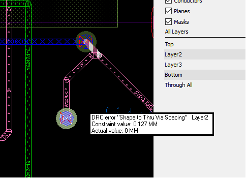
I observe the following error message:
DRC error "Shape to Thu Via Spacing" Layer 2
Constraint value 0.127mm Actual value: 0mm
Is this a problem with the via or the shape? Suggestions how to fix in constraint manager? Via editor? Shape generator?

I observe the following error message:
DRC error "Shape to Thu Via Spacing" Layer 2
Constraint value 0.127mm Actual value: 0mm
Is this a problem with the via or the shape? Suggestions how to fix in constraint manager? Via editor? Shape generator?

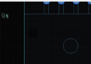
I'm trying to create a void in the Place Bound layer so that I can create a 3D representation of a hole through a mounting plate, but Allegro is telling me I can't add voids in that layer. Does anyone know of a work-around? I tried the XOR and ANDNOT shape operations, but I couldn't seem to select the round shape inside the plate outline that was meant to be the hole. See pic attached. Any thoughts?

I'm having trouble locating these constraints. I want to change the hole to everything spacing to 30 mil. I did it in constraint manager but when I update the dynamic planes the spacing is still 8 mil.
The mechanical pins do not have any constraints associated with them.
Hi All,
Are Cadence Allegro licenses only valid for a year or is there some for of license that would continue beyond the license period without updates or support?
I was wondering if it was possible to continue using Allegro beyond a license period without support in a similar manor to Altium or EasyPC?
Regards
T
I run Capture CIS on Win7, querying a MariaDB (MySQL clone) on linux. Recently, I upgraded the ODBC used to query the database to the most recent version (3.0 MariaDB connector), to upgrade the SSL security of the connection.
CIS started failing with SQL syntax error messages, complaining about names delimited with double quotes (instead of single quotes or 'accent grave' backwards single quotes), which is what MySQL and MariaDB want.
Yes, I had set the "Table Qualifier=`````` " etc lines in Capture.ini. I had it that way before the change, as well. Lots of thrashing around to try and fix it, and so I thought I'd share the problems and the (one, maybe two) solutions.
First, "base release" Capture 17.2 works fine with the "Table Qualifier" "Field Qualifier" entries in Capture.ini. However, more recent hotfixes (hotfix 33 and above, maybe earlier ones) FAILED. They ignored the "... Qualifier" entries entirely, always using double quotes to query the database.
It looks, as far as I can tell by dumping strings from near where "Table Qualifier" shows up in the code, that there is a new configuration variable "UseDatabaseProvidedQualifier". Not documented, didn't try it, but using it might be a fix.
A fix that *did* work was adding a SQL string to the ODBC connection setup:
SET sql_mode='ANSI_QUOTES';
Works for MariaDB, so probably works for MySQL.
Hi Folks,
I'm new in here and an ME with a long career in electronic packaging. So I've worked with lots of EEs and ECAD Designers in my career. But one thing I've found that hasn't seemed to change is that circuit heat dissipation estimates from the CCA design EE continue to be ultra-conservative. Too conservative for that matter! I've seen total CCA power estimates 2-3 times higher than measured in the final product in the lab (operating under worst-case duty cycles). But at this point in most design cycles it's too late to spin the design again to remove the thermal management hardware I added but rendered unnecessary by the lab measurements.
My question is this: does Sigrity PowerDC do this? If so, how and with what assumptions and conditions? Is there a whitepaper behind it?
if not, is there ANY software that will do a statistically sound power dissipation estimate on a circuit well before the end of the design process?
TIA!
Bruce
Hi I have an error trying to import my company's Access table to OrCAD CIS: Error is (ORCIS-6238) Part # property type not configured correctly in table capacitors.

I am very confused by this error, I'm not sure what it wanted me to do. Would anyone more knowledgeable here who has imported an Access database/table into CIS before be willing to help or make a suggestion, or see something in how I specified the tables here as incorrect? How do I configure Part Number correctly in access table, should it have been a Number instead of a short string?
Also and this is an aside but I am also very confused by the internet component assistor (ICA) and not sure how to get it to work especially based on this drop down. How do ICA database properties? Maybe there is a pdf guide that really is specifically geared toward the ICA that I just couldn't find. I've even seen some guides say ignore the ICA because it is obsolete.

Hey guys...any help would be appreciated. I am sure like with most things, the answer is super simple and staring me right in the face, but I certainly can't see it this morning. I am working on a Revision of an old design that was originally designed in v16.5 but is now being edited in v17.2.
I need to add two layers to this design and tweak a few of the thickness values, however, I seem to be 'locked' out of the ability to Add Layers. The menu item is greyed out and not selectable.

Is there a hidden switch to allow me back in to edit my Cross Section?
Thanks,
Thomas Miller
I m using ORCAD capture CIS v17.2 . I am not able to view the net alias by placing the cursor over it. When I select the net, the net name is displayed below. I was able to this in my previous projects. But don't know how the orcad setting has changed.
Please tell a solution.

Hi,
I'm drawing a schematic. I would like to add some property/constraint about some nets, for example, minimal/max width tracks or spacing.I have read on cadence Help that in Property editor window i have to change filter in "Capture-Allegro filter". But when i open Property editor window in de filter i have only "current property", I can't to choose another filters. How do I choose another filter?
Thanks in advance.
I am using Allegro 17.2 and I need to import some PADS footprints.
The footprints are given as four files, *.ld9, *.ln9, *.pd9, and *.pt9, how do I get Allegro to translate those files into a *.dra file?
The manufacturer gave me no other files, but Allegro seems to want to use a *.asc file or a *.ini file?
Thanks,
David
In Allegro PCB Designer, when I right click on canvas, all entries in context menu are show gray. They are all accessible and enabled but the text color are light gray and displayed as they are disabled.
Is it a new feature like I must select a specific mode? It it a known issue?
Thanks
Dear engineers
I have trouble with mass placing more than 10,000 parts since this operation takes too much memory.(File size is 1.06 GB)
Even though I could placing them all, because of huge amount of parts, the program woked too slow.
Are there any solutions to make this program more lighter of faster without upgrading my computer?
Or are there any options that make each part more lighter?
I really hope there will be a solution that I don't know yet.
I need your help..
Thank you
I made a four layer board. I also made a shape in layer 2 that I defined as ground (0V) I need to perforate the “ground” plane with vias to connect layer 1 to layers 3 and 4 without making contact with layer 2 (gnd). I observed the following error(s)
DRC error "Shape to Thu Via Spacing" Layer 2
Constraint value 0.127mm Actual value: 0mm
Where in constraint manager may I fix the following problem? Is this a problem with the "shape" or the "via"?
If this a simple fix, then please contact me and tell me what a foolish things that I have done.
.
Hi all,
I didn't find posts about this argument. I have to drawing some library about mechanical parts in capture Cis. I have files DXF about mechanical part. Is possible to import file DXF while i'm drawing a new library (capture cis)?
Dear All
I m an newbie to Orcad PCB Designing Suite & Application,
I hope I m not repeating the stuff again,
Earlier I worked on PCB's and PCB Designing through Ares, Due to user friendly nature it was very easy to design simple boards
Since I wanted to learn and improvise on my PCB design skills I m trying to get hands on, On Orcad/Allegro PCB Designing Suite.
Can anyone please post the Step by Step Procedure to add Jumpers and jumper property to orcad Pcb please.
I have tried creating "JUMPER" Footprints but I end up having errors saying the footprint is NOT An Jumper
Agreed that the easy way out is to add Vias and then replace the pad Stack of Vias to any required Size,
I hope there must be another good way around.
Kindly Guide me
Regards
This is something that has bugged me for a while and I have not yet found a solution:
we often re-use schematics in the form of modules. Typically, we create the module following a procedure similar to the one described here and, in most of the cases, the result is acceptable if a bit ugly.
What I mean is that the symbol created automatically is often very messy, with pins scattered more or less randomly, apart for the convention "inputs on left, outputs on right, I/O on top".
As I say, in most cases I prefer not to touch anything but sometimes it is necessary to rearrange the ports in the symbol, and this is where headaches start, because if I move the ports, I am very likely to get the dreaded error "Schematic has port but port does not exist in the symbol. Either delete this port from the schematic or add this port in the symbol." Even though all I have done is move the ports around, not add/remove anything.
The procedure I am following at the moment is this (Allegro 17.2-2016):
- generate the module using tool > generate view. This produces a symbol that I can re-use but very messy from the graphical point of view
- tools > library tools > part developer: open the cell I just created, and go to symbols > sym_1, click on the Symbol Pins tab
- from here, I click on Edit in Symbol Editor, which opens a new window
- in the symbol editor I can, in principle, drag the ports around. However this is where things go wrong, for some reason. In particular, it seems the issue is with ports named like XXX_N. They are automatically created with the bubble that indicates a "active low port". If I try to move any of them (drag them), I can save the symbol but when I try to place it again, I will get the error mentioned above.
Can anyone shed some light in what is the correct procedure to move ports in the symbol created from a module using the generate view functionality?
Shall I not use _N for naming pins? Am I supposed to use a different program to edit the symbol?
As always, any help is greatly appreciated.
Hi everyone
I'm looking for a format/standard/help document that how to form a netlist fie can be imported to orcad pcb editor for a developing program
I wanted to get a sample from my circuit, but when I go tools, the create netlist is grey. I tried a fulladder circuit but function still not available (((
Is there anything else I need to do to activate the function? if anyone can help me get a document about the format of netlist I will be even happier
thanks for listening to my problem
HIII Guys...I hv a small query regarding orcad capture symbol editor..As i create any SYMBOL the pins are not moving smoothly though i uncheck the SNAP TO GRID option in the settings..I disbale the GRIDS option too and tried other things but unable to resolve the issue..The pins of any IC i am creating doesnt moving smoothly...
I have done some test and seems that Pad Translator loose any swappability info of the components.
It generate always 1 gate containing all the pins.
Also all the pins are NOT swappable.
the sama appens from the translation from ALTIUM.
Is there a way to receive the correct device.dev. ????
Also when i try to translate the PADS Library the translator loose all the Gate definitions inside the filename.p
Any suggest?