Quantcast
Channel: Cadence PCB Design Forum
Viewing all 5525 articles
Browse latest View live

Place Bound being added automatically to symbol without one - 3D View

$
0
0

We are starting to move forward with associating STEP models to each library part for use in assembly drawings. This is working well except I have come across an issue I can't figure out.

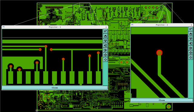
I have a footprint for a 125 mil dia mounting hole with a 250 mil pad. When this footprint was created there was no place bound defined for either the top or bottom. When I view the board using the 3D viewer, these mounting holes have a square box showing on the top side only. Bottom side shows the pad as expected.

Nowhere in either the footprint .dra file or the padstack do I have a place bound setup for this part. I even went back into the library editor and added a circular place bound for the top layer and when I refresh the part it shows BOTH! both the square AND round place bound.

What gives? Why would a place bound be assigned to a footprint that does not have one? I can delete the place bound shape in the board file and the part then shows correct in the viewer, 

Thoughts?

Tom

Using 16.6 latest SB

Smart value CLR feature in CIP-E database

$
0
0

Hi all,

I wonder if someone has used the smart value CLR feature for CIP-E database? I can't find too much documentation and the CIP database installation fails when I select this feature during setup.

Someone knows what this feature actually supports? I assume it supports improved value search when the value field contains suffixes(uF, mohm etc), but I am not exactly sure.

Ivo

Move components / block to new page, keep annotation?

$
0
0

Have a growing design. Need to split a schematic into two pages.


So, the pages are in the same schematic folder, and I just want to move some components from one page to another. I have checked "Preserve reference on copy" to no use.
In another ECAD tool I have used we simply moved a selected box from one page to another and case closed, any chance to get the wanted result here somehow?

Linux - PowerSI 2017 issues

$
0
0

Hello Everyone,

 Wanted to see if someone could help me resolve this issue below:

This is the error I receive when I attempt to launch powersi 2017 in Linux, the OS it's running on is SUSE 15.  I'm reaching out to the community here to see if anyone has seen this issue before and if so be able to provide some guidance on how to fix it. Any assistance is welcome, thank you.

home/linux/cadence/installs/SIGRITY2017/tools.lnx86/bin/../..//tools/lib/64bit/libstdc++.so.6: version `CXXABI_1.3.8' not found (required by /usr/lib64/libGLU.so.1) 

How do I change drill hole size for VIA on ORCAD layout 16 ?

$
0
0

I want to preface this by saying that I'm very new at PCB design so please bear with me .

The error I received from FAB manufacturer was this:" 

While performing DFM validation we observed that under size copper pads provided for all 12Mils via holes. Attached snap shot for your quick reference. Here the annular ring results zero mils and will lead to break out. Please provide sufficient copper pads to have sufficient annular ring (at least via size + 6Mils )and resend the updated gerber data."

I don't fully understand what the problem is and how to fix it.  Should I be able to see the drill hole on the layout?  From what I understand I need to ensure that the via sizing is such that it has at least 6 Mils clearance from the drill hole. I am able to increase the VIA pad size but im not sure how to alter the drill hole in ORCAD LAYOUT.  I was thinking of adjusting the pad sizing for either DRLDWG or DRILL layer, but I'm not sure what the difference between the layers are. Thanks !

Cadence Allegro 17.2 - Shape to board outline clearances.

$
0
0

Hello all,

I hope you can help, I have different requirements for clearances to the board edge which I want to enforce.

For example one net can have copper 2mm from the board edge whilst another has to be 4mm away.

How can I control this automatically in Allegro ?.

At the moment I have two draft lines which I follow manually, I'd like Allegro to do this... and DRC !.

Thanks for your time,
Chris

Print pdf with Orcad 10.5 search for a word

$
0
0

I have a problem whit "the old" Orcad 10.5. I need to print a pdf file about silkscreen layer. I know as print the layers but I don't find the option " Non-vectorized-text ". I want to be able to search for a word in the pdf file. Do someone know as to fix this problem? Are there other modes? 

Thanks

Orcad Capture - Display multiple Attribuites

$
0
0

Hey guys...this is either so easy I am missing the obviousness of it or it is some obtuse Capture'ism that I can't figure it out.

On my Capacitors on my schematic, I would like to be able to see BOTH the Value and the Voltage. I can make this happen easy enough in the schematic, but I would like these Attributes to be a default in my library so that anytime a new capacitor is placed, I see both Attributes.

As far as I can find, at the library creation level, I can't add additional attributes or Basic Attributes.


How to change Copper pour spacing in PCB layout for ORCAD layout

$
0
0

I was wondering how I could change the copper pour spacing because i recently got an error saying that for several layers, the spacing is too little between pads and ground layer. 

Via Structure on Bottom Layer

$
0
0

I can create Via structure on top layer by open "Route>Via Structure>Create>Standard" and then use fanout tool to add it to my design. 

But for bottom layer I follow same routing. create a trace on bottom layer, create the Via Structure and use fanout.tool but I cannot add Via structure on any bottom pin.

ERROR:

E- (SPMHGE-633): Library via structure BOT subclasses don't match to command parameters. Via structure can't be used.

I Know that starting layer should match with Via Structure and I verified that my created Via Structure is on bottom nevertheless I get the error.

Please heeeeeeeeeelp. I have more than 1000 pins that need this fanout!

I Use Allegro 17.2 HotFix 042

Tested Via Structure

community.cadence.com/.../bot.xml

STEP model mapping

$
0
0

So when trying to map a STEP model to a footprint it works fine, however whenever I try to use that footprint on a board layout the STEP model is no longer attatched and I have to re-map the STEP model to the footprint (this time in the board layout) is there any way around this? To just map the step models ONCE to their footprints and never have to re-map them again?

How to make a shared prefprops.txt file.

$
0
0

Hi,

When using the Edit Object Properties spreadsheet in Capture 16.6 I would like provide some new drop down filters to all users.
If I change the PrefPropPath variable in a local Capture.ini file to point to a central prefprops.txt file I find that this only works if
that file is writeable. If the file is readonly then it is ignored. This means that all users would be writing to the same file which
would not be a good idea.
Is there a better solution?

Thanks,

Jim O'Mahony

Copper Pour Clearance Clarification

$
0
0

In Orcad Layout, I am wondering what the clearance option for Copper Pour Rules,in the edit obstacle menu,  means and what happens if I decide to change the clearance option? Does changing the clearance option increase the distance between traces and vias to that particular copper pour area or obstacle ?  


Rules Checker HDL error trying to compile custom rule

$
0
0

Hello,

I've been trying to create a custom rule (actually any custom rule) and get it to compile, but I get the following error in the .log file after compile.


**Error! [5006] Could not find '-r'
I assume this has something to do with the cp.dat file: 
Here are its contents:
-e
-r "%CDS_SITE%/tools/checkplus_exp/concept/env/logical_env.rle"
-r "C:/temp/customRules/eight.erl"
Thanks in advance for any ideas!

Orcad Capture - Error 5004 (Netlist export / Error intializing COM property....)

$
0
0

Morning,

I don't fire up Orcad very often, so I can't say when this issue started happening. When I try to export a netlist of a design, I get the error:

ERROR(ORCAP-5004): Error initializing COM properly pages: Invalid pointer

I've tried the solutions presented in this post, but neither of them work. The "regsvr32 orpxllite.ocx" results in a further error:

"The module orpxllite.ocx failed to load.
Make sure the binary is stored at the specified path or debug it to check for problems with the binary or dependent DLL files.
The specified module could not be found"

I also tried running the provided debug .TCL script from that post, but it gives no return at all.

Running in Admin mode does nothing to change the result, same error.

I'm running 16.6.-S086 (v16-6-112HJ)

Any ideas to fix this?

Thanks,

Rafael


pinpair-Min/Max propagation delay

$
0
0

hi

i'm creating pin-pair in min/max propagation delay, actually nets travel from U1 to J24 to R215. after crating pinpair  from  U1.C21 to J24.124  only .after Right click select Analysis option Automatically pin pair added from  R215.1 to J24.124. Please explain this issues why its coming  images attached .

Thanks

How to export logic from PCB editor?

$
0
0

Title says.

Is there anyway I can visually see the logic of a board file? I'm using a generated netlist to feed PCB editor but no design file. A pity to be sure that I can't export .brd into capture

While updating footprint, the shape symbol is not updated automatically in cadence Allegro 17.2 tool

$
0
0

Hello,

Recently I faced error in paste mask layer. while updating the footprint Ex.from 0402 to 0201 package, the footprint is updated but the shape symbol of padstack is not updated correctly in cadence 17.2 tool

Ex: The error shape symbol of paste mask for SMD_R0201 package

After update the shape symbol through Place --> Update symbols--> Shape and Flash symbols-->S_R0201_S3 (Shape symbol name)

Here My question, it is not updating automatically while updating the footprint?

Do you have any solution If it will update automatically while updating the footprint?

OrCAD Capture Data Tip customization

$
0
0

Hi,

I am using Orcad Capture 17.2 version. When i hover my mouse over a component in a design, i get a data tip pop-up displaying the part ref and value. Is there anyway i can customise this to add few more attributes to display, such as footprint. 

Kindly help me on this.I have attached a screenshot for more information.

Regards,

Chadga

Hierarchical ports moving around when adding and the synchronizing up...

$
0
0

I am experiencing that all hierarchical ports move about after adding one at the schematic level and then traversing up and then performing a synchronize up.

The ports also changes direction to "IN".

The only solution to this has been to lock all existing ports in the block before doing a synchronize up.

Am I doing anything wrong during instantiation or is this normal to the Capture module? 

Viewing all 5525 articles
Browse latest View live


<script src="https://jsc.adskeeper.com/r/s/rssing.com.1596347.js" async> </script>