Quantcast
Channel: Cadence PCB Design Forum
Viewing all 5525 articles
Browse latest View live

Calculating trace current .

$
0
0

Hi,

I previously used and IPC 2221 calculator for calculating trace widths for internal and external layers. I then started using Saturn PCB Toolkit since it used IPC-2152 to calculate the trace widths.

recently I did a board where the customer used the IPC-2221 to provide values for trace widths and I used the Saturn Toolkit. The inner layer widths came out so much smaller that I started to question the calculator.

I then read a number of articles and it looks like the IPC 2221 is very old and the inner layer calculations were just a guess at double the values. The IPC-2152 actually did testing on generating there charts and also

came up with the plane layers help in reducing the current. So perhaps the inner layers can handle more current ?

In doing more reading and looking at the manuals it looks like the Saturn calculator can produce IPC-2221 values. IPC 2152 without modifiers, with modifiers and with modifiers with planes.

Also I bought Ultra-cads calculator just to check the Saturns result.

So I have a IPC-2221 calculator , two IPC 2152 calculators , a number of IPC-2152 charts and  a spreadsheet with various results from all the calculators.

I do not believe the Saturn calculators values for IPC-2152 are accurate as they are different than the IPC 2152 charts. Need to do more comparisons on the ultracad calculator to see how close they are to the charts.

Just curious of what others use and of they have any experience with the IPC 2152 Calculator ?


How to force annotate to increment only the two last numbers of a component

$
0
0

Hello,

I am using Allegro Design Entry HDL version 17.2-2016.

We have a pretty big design (42 pages), and we have a company directive that says to set the numbering of each component to 4 numbers, the first two numbers corresponding to the page number.

For example, all resistors of page 6 will start as R06xx, being xx the number of resistor on that page. All capacitors presents in page 15 will start as C15xx, being xx the number of the capacitor on that page.

I am using scripts to reset the LOCATION property to $LOCATION=R? in order to restart the resistor naming (auto property a $LOCATION=R?).

However, is there a way of setting this to, for instance, $LOCATION=R06xx in order to tell Allegro to set only the last two numbers of the component?

Best regards,

Daniel Tormo

Capture slow/laggy UI response

$
0
0

I am having a very slow response to Pspice schematic capture ever since upgrading to WIN10.  It takes about 1sec from clicking on a component before the UI selects the part.  The response is not "fluid" as when using on WIN7. 

I am using  Microsoft Windows [Version 10.0.16299.904]

Crossprobing between concept HDL & Allegro PCB Editor

$
0
0

Hi Anyone,

i'm using concept HDL for schematic & allegro for PCB design.i need to select multiple items using cross probe.But I can select only single component at a time in HDL for allegro.Can any one help me how to select multiple components in HDL so my work will be easy in PCB

PCB Footprint Physical Changes Update report

$
0
0

I am using OrCAD PCB Professional 17.2. I create footprints and manage the libraries. One of the designer has made changes to the orientation and naming of pins in the footprints while designing the board. After gerber generation during reviewing we got to know this. I need to know what changes are made to the footprint as the designer didnt update us this info. Is there any report which we can get for the changes made? Or can we compare the updated footprint in the board with the origianl one that of library? 

With schematic parts we get the details of the properties changed for a component in Part Manager. Is there a way to do the same for footprints as well?

Kindly let me know how to avoid with these kind of issue.

Cadence Sigrity Simulation

$
0
0

Hi All,

I designed the PCB in the Altium Designer 18. I imported this PCB in Cadence Allegro17.2-2016 for Simulation. I applied the DC Net & assign the values to discrete components. Then i save the project in *.brd file. For sigrtity simulation the conversion from .brd to .spd format is required. But i didn't find the CAD Translator for spdlinks. Please tell me how can i convert the .brd file into .spd for simulation.

I also attached this document that i searched on one of the Internet blog, but again its didn't help me.I didn't find the extracta.exe file. I attached this document for the reference.

Please help me out in this regard.

community.cadence.com/.../Allegro-to-Sigrity-Conversion.pdf

Error processing 'J6': Cannot modify element; the object or a parent has the FIXED property. ------The item does not appear to be fixed.

$
0
0

Hey guys, 

I've seen this one posted a few times, and I don't seem to be finding a fix that works for me.    When trying to make a new netlist, I am always met with this error.  I've gone into PCB editor, made sure it wasn't fixed.


#1 ERROR(SPMHNI-175): Netrev error detected.

ERROR(SPMHDB-195): Error processing 'J6': Cannot modify element; the object or a parent has the FIXED property. [help].


If the object is not fixed, and i'm getting this error, where do I even start?

part.ptf failure

$
0
0

the part.ptf is failing with the below warning, I have been trying to add the manufacture part number to the bom export. The schematic was exporting to the brd file and updating the brd file. The export was successful until the the ptf was created. I am looking for the ability to have the BOM be automatically created and a successful export.

FILE_TYPE = MULTI_PHYS_TABLE;
PART 'SMP_GAC_OPTIMIZED'
{========================================================================================}
:MFG_1         | MFG_PN_1       | MFG_2   | MFG_PN_2 | DESCRIPTION | VALUE | PART_NUMBER | PART_NAME(OPT='SMP_GAC_OPTIMIZED')   =  ;
{========================================================================================}
 'Rosenberger' | '19S103-400L5' | "'def'" | "'def'"  | 'SMP'       | 'SMP' | "'def'"     | 'SMP_GAC_OPTIMIZED'(!)               =  : MFG_1 = 'Rosenberger' , MFG_PN_1 = '19S103-400L'
END_PART
END.

Auto-route in Cadence PCB Designer

$
0
0

Hello everybody!

I often use Bundle Create function in my .brd projects to highlight specific rats which are prior for routing. 

Is there a way to automatically route a Bundle that I created?

I know that you can autoroute rats, filtering them by net names or components, but it seems strange that there is no simmular function for bundles.

Allegro PCB Designer 17.2 with hotfix 49 is used. 

Every suggestion is helpful, thx. 

Set default net name in drop downlist

$
0
0

HI Guys,

Is there anyway we can set few default net name in drop down list as highlight?

Eugene

Importing DXF file as board outline deletes everything - 17.2

What's New hotfix 051

$
0
0

Hi guys,

I searched on the Cadence website, but I didn't find what I was looking for.

I see that HOTFIX 051 is now available, is there a link to any documentation to show what was updated etc ?.

I need to pass some information onto the engineering team, to let them know why they should update... and loose 15 minutes of their day waiting for the install.

Can anyone help with this ?.

Thanks,

Chris TAIT

Can't move 'unfixed' component, and mechanical pins disappearing.

$
0
0

Hey All, 

Ran into a new problem, and after an hour of googling, I am no further ahead.

I posted recently about updating an old board with a new connector, and how i'm a newb.   Well, I believe I have completed the changes on that particular board! Everything was great.  Now, I need to replace the exact connector on a different board.   I already have the part from the last job, and went about the process the same way, but this time, there's new problems.


I am now at the point where I have the new connector in the new .brd file, but the first thing I notice is that it's missing it's mechanical pins.    This is NOT the way it appeared in the last file.   Where did they go?

And secondly,  I cannot move this connector into place on the board.   As best I can tell, no part of this is "fixed" in place.   I click the "unfix" button.  I tried right clicking and selecting "unfix" and i've also tried it from the properties.

This is INSANELY frustrating as i'm doing it exactly the way I did it last time, and there is no indicator on the screen anywhere that's telling me why I can't do this.   Why can't I move this unfixed part?

Generating Capture BOM in excel gives inappropriate rows and column

$
0
0

hello ,

Generating Capture BOM in excel gives inappropriate rows and column, some of my component's property are shifted in below row as shown in screenshot see component J5

Quickplace - place components by room

$
0
0

Hello, I am trying to use rooms to place components on my board. I created a "power" room in the schematic and generated a new netlist. I imported the new netlist and placed my "power" room in pcb editor. Then I went to place --> quickplace and selected place by room. But the drop down that should show all my rooms is empty so I am not able to place the components.

I also tried selecting "place all components" using quickplace, but the viewlog says "placed 0 out of 0 applicable (0 total) symbols". Any ideas on why quickplace is not working?

Thanks!


Triangle Symbol on Differential Pair Signals

$
0
0

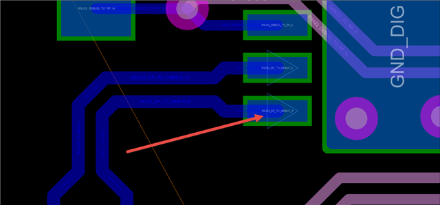
Does anybody know what this triangle symbol is for?  Been doing differential signaling for years and have never seen this symbol. It doesn't appear above any other pair, except this pair.

What is the difference between LOCATION and $LOCATION

$
0
0

All,

What is the difference between LOCATION and $LOCATION? 

I find nothing in the Cadence documentation, except saying that both are predefined attributes.

R.

EDIF Importing issues in Capture

$
0
0

Hi Team,

Greetings! I have a query regarding the EDIF design import in Capture.

When I try to import the design with the standard procedure(File->Import EDIF Design) it shows the below Error and Warning.

//*

EDIF 200: Reference Error: source line 829570: Identifier DDR_VTT NON-UNIQUE. Changed to DDR_VTT_0. Now it cannot be referenced!
..............................................................
..................................................................
EDIF 200 parsing finished
Could not find C:\CADENCE\SPB_DATA\
Library C:\mysys\DESKTOP\CHECK_CSK\BUILTIN.OLB is created
Library C:\mysys\DESKTOP\CHECK_CSK\TS6370K_PRELIM.OLB is created
Library C:\mysys\DESKTOP\CHECK_CSK\TS6370K.OLB is created
Warning: Optimal grid cannot be selected. Net Graphic can change
Error: Cannot determine grid. Please, try setting grid by command line option
Fatal Error:  in OrCAD Writer:  Cannot determine grid. Please, try setting grid by command line option
Finished on Wed Feb 13 16:53:47 2019
Fatal error detected
Could not find C:\mysys\Desktop\check_csk\TS6370K.DSN
Could not find C:\mysys\DESKTOP\CHECK_CSK\TS6370K.DSN

*//

Note :  

I have imported the same .eds file with 16.6 AND  17.2 versions both are giving the same.

I would like to know what are all the possible ways to fix this issue and let me know how to fix them.

Thanks in advance.

dv.

Capture CIS Database File Read Only Issue

$
0
0

We are working with OrCAD Capture CIS 17.2. I am a librarian who populates the library data onto an Access .MDB file and all the Libraries sit in my PC. When Captuer CIS is opened in the Client PC, and later I try to open my Database file to add new components, I get a Pop-up telling it is in use and can be opened as Read-Only. 

Now If I want to change or add anything to the database file, I have to close all Capture CIS tools and then do it. Is this how it is usually done? Or is there any way to configure the database where we can edit database file and use Capture CIS simultaneously?

Fill the unuse area with copper in panel

$
0
0

Hi Guys,

Any idea how we can fill up copper on the unuse area in panel, except send to vendor and ask them do it for us..

I able to do that by playing around the route keepout and keepin and then import the sub drawing back to original board file but it really take time.

Hope to get some input from you guys.=)

Regards,

Eugene

Viewing all 5525 articles
Browse latest View live


<script src="https://jsc.adskeeper.com/r/s/rssing.com.1596347.js" async> </script>