Quantcast
Channel: Cadence PCB Design Forum
Viewing all 5525 articles
Browse latest View live

Can I link a inductor part to resistor part by using CIS variant design?

$
0
0

Hi there,

There's LC input filter in my design, but I want to use 0Ohm for the inductor first. I tried to use variant design, but the part manager does not allow me to link a resistor part to a inductor part. Is this possible in Orcad CIS?

Part manager says: "Cannot link database part on this variant because the schematic parts differ".

I think this is a reasonable function for variant design...


17.4 Design Sync, parts without footprint

$
0
0

Hello,

I just installed new 17.4, and tried to start using it. I was really hopeful about the new Design Sync-feature since I've always found it quite cumbersome.

Anyway, I immediately ran into problems.

For several years, I've been adding extra parts to schematic to get them into BOM (such as screws, light pipes etc) by not assigning them any footprint or pins.
With old way of doing things, these parts has simply been ignored in netlisting, causing them not to end up in PCB (which is what I want).

With new Design Sync function, I end up with error message "WARNING(ORCAP-36050): No pins are present in Z12. Ignoring this component in netlist." Although the *warning* is not treated as a warning, it has severity *Error*, causing function to fail.

Also, the old way using netlist doesn't seem to exist anymore? No way of automatically update board that way, so 17.4 is basically not usable as is?
No, I don't want  to resign to removing these parts from the schematic.

Silkscreen(Refdes) Alignment

$
0
0

Hello Everyone,


I am looking for an option to align silkscreen text (Refdes) in a row and column.


Is there any option for silk screen alignment(Refdes) as like “component dynamic alignment” ?


Is there any way to check by running some skill scripts, such that to ensure Refdes silk screen nearby components with in specified distance?  

Thanks & Regards,

Amrutha CV  

United Kingdom 17.4 Orcad Users

$
0
0

Hi All,

Having downloaded and installed orcad version 17.4 I am ready to "play with the new features"

however I am still waiting for my new Licence file. I have contacted my distributor who informs me that they are waiting for Cadence to release the

keys.

Is there anyone else in the United Kingdom that is waiting for there licence files.

This is frustrating I actually downloaded it nearly three weeks ago but still no licence file I have checked my junk email bin to make sure it hasn't found its way

in there.

Altium to OrCAD 17.2 Translation Issues

$
0
0

Hello all,

I have an issue for which I cannot find a solution.

I have translated an Altium schematic using File->Import->Altium Schematic Translator. Under the dialog box, there is a help file that explains what needs to be done in both Altium and OrCAD. I saved the files as the Advanced Schematic binary (*.SchDoc) as directed. There is a PCB Project file (*.PrjPCB) and a valid structure file (*.PrjPCBStructure). I converted all of the Altium schematic pages to custom so the page sizes will be correct. Almost everything translated properly except the few things that is indicated that it cannot understand such as the signal harness where the signals are combined into one fancy line. That is not an issue for me at the moment. The main issue I have is the non-aliased nets reverted to an OrCAD default naming style, something like N00027 from say Q6_1. This is not necessarily a problem either. I know that OrCAD capture cannot change the names of the nets back to the Altium style.

The problem that I know I will have is when I try to link the PCB to the schematic. I know that I will have to re-run the Tools->Create Netlist... to recreate the netlists. This will be the problem. When I translated the Altium PCB to OrCAD, I followed the same instructions that were found Import->Translators->Altium PCB.... The help file under that dialog box explains that you need to save the PCBs as a PCB ASCII File (*.PcbDoc). I checked the Create Individual Symbol Definitions and Derive Connectivity check boxes as well as the Extended radio button. The board was completely translated. All of the traces/nets were translated as they are on the Altium PCB.

The issue that I have is the translated PCB nets do not match because none of the non-aliased nets changed into a default net like in the schematic. So the question is, how do I change the PCB to make the traces/nets conform to the schematic net naming so I can recreate the netlists?

Any help would be greatly appreciated.

regular pad flash and odb++ output

$
0
0

We flash a 5 mil pad on the top and bottom layers for a non-plated hole.

A larger pad is there in Allegro 17.2 to keep copper away from the hole.

When we gerber out, the large pad is replaced with the 5 mil pad that gets drilled away.

We cannot get ODB++ out inside Allegro to make this substitution.

Is anyone doing some thing similar ?

Thanks

Les

How to define via structure in allegro /Orcad 17.x

$
0
0

Hello

I just migrated from 16.x to 17.x , finding difficulty in Defining via structure .

in 16.x it was easy "select Cline,via and create via structure and then click on fan-out use the defined via structure for similar type component "

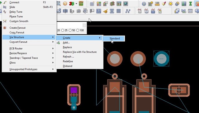
Now in 17.x  its saving in .xml format and when go for fan out define via structure its not available from the drop down menu . I am not clear with preserve property  (refer image)

Anyone could help me on this ?  I googled it but didn't get proper explanation  (community.cadence.com/.../highspeed_5f00_via_5f00_structures)

Thanks

GK

Altium to OrCAD Schematic Translation Page Name Truncation Issues

$
0
0

Hi All,

My client's Altium schematic pages have names that are longer than 31 characters. After translation, the schematic page names get truncated to 31 characters. Is there a way to prevent this and allow the full size schematic page name to be there? I saw in a posted response by oldmouldy in this post: https://community.cadence.com/cadence_technology_forums/f/pcb-design/24284/translating-a-layout-pcb-character-length indicate that there may be a way to do that but I cannot find it for OrCAD Capture CIS. I also think I found a post a while ago that indicated that I would really need to do it in the command line when executing the program but alas, I don't remember what that post was referencing so I cannot find it again. Any help would be greatly appreciated.


In Allegro 17.4, many long character net alias cannot be displayed on a pad or trace

$
0
0

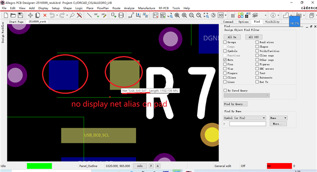
bug #1  In Allegro 17.4, many long character net alias cannot be displayed on a pad or trace        

bug2    And all of the pads and the net alias shown on trace are blurred(sawtooth) after zooming in, which was not the case in the previous 17.2 version....

In the footprint viewer of OrCAD 17.4 Capture, the zoom in, zoom out and zoom fit buttons have no function

$
0
0

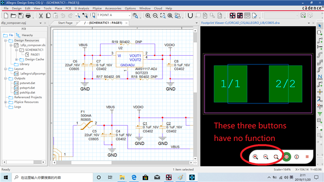
In the footprint viewer of OrCAD 17.4 Capture, the zoom in, zoom out and zoom fit buttons have no function

In allegro 17.4 (1366*768 Screen resolution ), the User Preference editor dialog box can't display OK or Cancel !!!

$
0
0

Under the resolution of 1366 * 768 computer screen, the User Preference editor dialog box cannot display the option of confirming at the bottom corner

In OrCAD 17.4, there is a problem with using file -- Print

$
0
0

In OrCAD 17.4, use file -- print, and then choose Adobe PDF or other printers to print the schematic diagram. As long as a page of the schematic diagram is opened, the opened page will be abnormal after printing, and selecting horizontal center and vertical center will not solve the problem

Reset OrCAD Capture and PCB Editor to Default Layouts Version 17.2

$
0
0

Hi All,

How do I get the OrCAD Capture and PCB Editor to reset to the first install layouts? I tried this: https://community.cadence.com/cadence_technology_forums/f/pcb-design/29010/default-toolbars-in-capture-cis but it did not work. I removed a window that showed some kind of information. I don't believe it was the Command Window because there was no text label on the side of the window like what is displayed on the Command Window. After trying what is in that link, I get a brief glimps of the window but it keeps disappearing. Any help would be greatly appreciated.

Allegro .men file conversion to .il menu file

$
0
0

Hi All:

How do you go from using custom .men files to the new .il menu files ?

Thanks

Les

Finding duplicate reference designators in Concept HDL schematic

$
0
0

Hi,

we have imported few pages from other design to current design.

Because of that we saw few reference designators are duplicated.

1. How can i find duplicate reference designators? 

Based on the number of entries i need to see whether i can manually change them or is there any way to do it automatically. 


Placing and routing identical circuits in PCB

$
0
0

Hello,

I'm using OrCAD PCB Designer Standard version 17.2-2016 S056.

I have few identical circuits that need to be placed and routed in a similar fashion.

Lets say I placed and routed one group of components and I want the second group of components to be placed/routed in the exact same manner. 

Groups have same number of components. 

Thanks,

Santosh

17.4 Exporting a brd to Specctra Router Issue.

$
0
0

Hi guys, maybe someone knows something on this.

In 17.4 " File > Export > Router" is not working for me. The command Window returns the following error

"Command Not Found Specctra_Out"

Taking a different approach using the utility "PCB Editor to PCB Router 17.4" I get an error

"Cant open Router Setup Form (VSE_ARMAIN.FORM)

i May save a call to tech support if anyone knows of a fix for this or can confirm Specctra out is working or not.

Specctra will launch, just can generate a .dsn file for it.

Thanks

17.2 Allegro PCB Librarian XL : Part Developer

$
0
0

After loading hot fix 059 there seem to be a few changes to the Allegro Part Developer.

The biggest change to me (and I'm not sure if I am missing some setting or not) seems to

be not seeing the symbol when choosing a symbol in the package/symbol tree. Is there

any way to have that be visible? Also a radio button with "Edit in Symbol Editor" that is

new. Any way to have that default to open in DE-HDL ? Another thing that seems new is

a RMB on a sym having the ability to open in DE-HDL or In Symbol Editor.

The big thing for me is to have the symbol viewable when viewing the "Symbol Pins" tab,

otherwise things like Set Origin or changing pin graphics are useless.

Symbol editor missing property sheet tab/drawer

$
0
0

I am using capture 17.2.2016.

When i use the symbol editor i can not see the property sheet drawer / tab to edit pin properties.

Is that a feature available only with a certain license or is something broken with my capture installation ?

What do i have to do to see the property sheet drawer / tab?

i would like my symbol editor to look like this...

https://www.orcad.com/resources/library/symbol-editor

mine currently looks like this..

Re : Planarity of ATE socket Mounting & Donut pad of socket

$
0
0

Hi ,

Can anyone explain the purpose of maintaining "planarity" for ATE test socket and purpose of Donut pad?

Viewing all 5525 articles
Browse latest View live


<script src="https://jsc.adskeeper.com/r/s/rssing.com.1596347.js" async> </script>