Quantcast
Channel: Cadence PCB Design Forum
Viewing all 5525 articles
Browse latest View live

Soldermask and Pastemask Layers

$
0
0

Hi All,

I've just about to finish my first PCB layout, and I want to understand some 2 issues better:

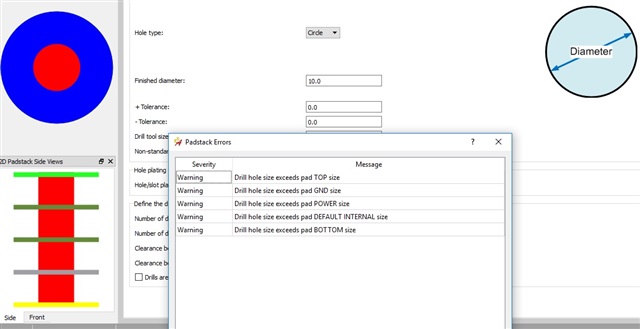
1. Soldermask layer: when exactly do we want to define for some SMT pad (say at Pad Designer tool), to have soldermask top and when we want to define solermask bottom

if it's a TH pad, I guess we always want to define both layers soldermask (top, bottom), because the pads are crossing all the layers. However, if it's a SMT pad, which SM we want?

2. Pastemask layer: is this layer necessary for the gerber files generation, when we have SMT components in our circuit?

And again, when we define for a TH/SMT pads pastemask top, and when Pastemask bottom?

Thanks!


Advance Annotation error

$
0
0

Hello all,

We are designing a backplane and in the design we are using some custom prefixes using the Advance Annotation tool. When annotating the occurances I get the following error:

ERROR(ORDBDLL-1224): The total number of components for prefix J0C exceeds the range supplied for it.
Increase the End value of the range.

Thanks in advance for the help

--Tom

ORCAD 17.2 Win 10 Install Error

$
0
0

I'm trying to re-install ORCAD 17.2  in a PC from a DVD which I have upgraded from Win 7 to Win 10 and  now has a new 500GB SSD. While installing I got a Windows Application Error  0xc000007b. When I try to run ORCAD I get the same Error.

Looking for ways to fix this problem.

New comer, need help with VIA drill size change

$
0
0

Greeting to all:

I am new in this tool, only 2 weeks. Trying to create a new Via with smaller size drill hole from exiting 13 mils size to 10 mils size. I got the message as imaged below. Any advise what to do?  Thanks in advance.


Is it possible to find or create a Pspice model for the JT3028, LD7552 components?

$
0
0

I would like to add these components to the component bank in ORCAD simulation. Even an accessible or free course that explained how to create these components.

Create a new Constraint Group or Constraint Class ?

$
0
0

When in Constraint Manager, Physical Domain, one can create a new Physical Constraint Class defining specific attributes for a custom rule set. One can then assing this new rule set to a set of nets. To do that it is instructed to create a new Net Class with menu Objects > Create > Net Class. Also on that same menu is available Net Group. Both options create a group that appear in the Constraint Manager Objects Name Column. I have triied both  options and cant really see the difference. 

The Question: What is the difference between creating a Net Class and a Net Group ?  What are the implications ?

Thanks for your help.

OrCAD PCB Designer Pro w/ PSpice, Design Object Find Filter Greyed Out

$
0
0

Hello All,

I'm currently using OrCAD PCB Designer Professional w/ PSpice (version 16.6-2015).  In the 'Design Object Find Filter' side bar, all options are grayed out and unselectable.  I did attempt to 'Reset UI to Cadence Default' without any luck.  A colleague has no issues with the identical file on his computer.  Any guidance would be much appreciated.  Thanks!

George

Custom pad shape and symbol, when placed on pcb pad locations move.

$
0
0

Hi everybody,

I've created a symbol with custom pad shapes. Everything looks correct in the symbol editor.

And the 3d view looks correct (upside down to show placement)

But when I try to place it on the pcb the 2 "T" shaped pads aren't in the correct location.

I have the pad shape centered on the pad...

with no offset on the padstack editor.

Does anybody know how to fix this?

Thank you!


Allegro PDF

$
0
0

What are folks doing to create PDFs that include artwork (shapes and routes) with Allegro? Everything I tried results in a terrible quality pdf. "Export PDF" resulted in awesome pdfs, but since that went away I've been struggling. I do a lot of work with die attachment and I need a lot of detail. We are currently stuck with Nuance for a pdf tool. I do not have admin rights, so I don't have the luxury of downloading and trying out different tools. 
Is Cadence going to add the PDF export option back any time soon?

Thanks

Allegro design entry DHL, pin swaps , export without exporting constraints, back annotate.

$
0
0

Hi,

I have a new customer that uses Allegro Design entry HDL for the schematic and have a few questions.

1. How do you get pin/gate swaps into the symbols in the schematic ?

2. How do you transfer them to the pcb editor ?

3. How do you back annotate the swaps from the pcb editor to the schematic ?

4. How do you stop the export/Import physical from updating the constraints in the pcb file ? 

Capture BOM wrong

$
0
0

Hi

i have generated a BOM of my design and one of the parts is showing wrong information than what I specified in the database. I can see that in CIS database that part has been specified a correct information  but when I exported it to bom it shows wrong values.

Orcad CIS Variant Bom Missing

$
0
0

Hi There,

The variant bom I set gone dissapear. Is there any way to recover this back from the old design file? 

This is the second time it happen to me. Not really sure what could cause this. 

Thanks,

Pornchai

trace ends from round to square?

$
0
0

Is it possible to change trace ends from round to square? Allegro PCB Designer 17.2 (basic)

Thanks

Why is my grid changing when I add connections or sliding connections in allegro 16.6?

$
0
0

Some little time ago I was editing a pcb layout and I deleted some tracks and I redrew them with a grid that I set to 0.1mm.

Now, I don't know why, when I click "add connect" or "slide", grid points distance grows automatically.

When I go to setup grid I can see that grid stills 0.1mm, but grid distance on my project canvas is about 10mm (I saw that with "show mesure" tool).

So now I'm unable to edit my tracks because I can't draw them easily with this 10mm grid, following the path that I want.

Is this a bug? Why is the grid changing this way when I click "add connect" or "slide connect" tools?

How can I solve this. I was drawing fine some days ago. Maybe some configuration parameter that I'm ignoring?

Why would PTH padstacks with flash symbols defined not be recognized within a board file?

$
0
0

 I have been assigned to finish a PCB design with dynamic shapes on both negative and positive artwork layers.   The thermal flash symbols are not recognize within the board file when creating a dynamic shape on either positive or negative artwork layers.  

When using the padstack editor the thermal definitions are being translated into being a rectangular void of X by X dimensions as if the thermal .ssm file is not accessible.  

I know these padstacks are valid as they are being used on a second design with no issues that mates to the design with the problems.     I verified that the global shape params are not different between the designs.  There are no difference in net properties between the designs.  

Please help.

Its got to be something simple, right?

Thanks,

Doricini


IDF Export to Solidworks (Holes not appearing)

$
0
0

I've been generating IDF and PTC for Solidworks import but plates/non-plated holes are not importing. I've tried with/without filter, and version 2.0/3.0.

I have been having trouble with both pins and vias (I have only included the vias as a test). If I open the emn or ldf, I can see them defined.

Could "ECAD" designation versus "PLACED" be an issue? I don't know how that is determined

MEC_HOLE0320CU0800_CL6 MEC_HOLE0320CU0800 PH7
55.0000 194.2000 0.0000 0.000 TOP ECAD

I get the following warning, as well

WARNING: More than one place bound shape defines the outline of MEC_HOLE0320CU0800_CL6.

  An overall place bounding box was exported instead.

vias -->

.DRILLED_HOLES
0.2500 -36.1250 34.6250 PTH BOARD
0.2500 -35.2274 34.5000 PTH BOARD

Same Net Spacing: Shape to Shape

$
0
0

I have a big shape covering the entire board and a small shape inside. Both shapes belong to the same net. The same net spacing is turned on in the Analysis Mode dialog and the Enable DRC By-Layer is set to TRUE, but the setting doesn't take effect. The shape-to-shape same net spacing is set to 0.2 mm. This example is, by the way, just for testing the constraint. Is there an additional setting that I have missed?

I would have expected this:

/F

How do I turn off snap to grid in PCB Designer

$
0
0

Quick Question, I can not figure out how to turn off snap to grid when placing components manually in PCB Designer. I am trying to align ann external connection component to the PCB edge but it either sticks out too far or is too far back on PCB. 

THANK YOU

How do I move my entire project in PCB Designer

$
0
0

Quick Question, I didn't realize when I placed the board outline that it was so close to the edge of my region. I am now trying to move a potentiometer footprint that hangs over the edge but I can not move it as far as I need. 

How can I move everything up in my workspace?

How to move component so that the pad aligns to the pad of another component (like Altium does)

$
0
0

When moving a component, is there a way to make the pad line up with the component pad it is connecting to ?

For example, with reference to the screen capture below...

I want to route a straight track (net +1V2D) between the capacitor (on the left) and the processor pin (on the right)

Therefore I want to move the capacitor (vertically down) so that the pad aligns with the processor pin.

I have a grid setup and use the capacitor pad as the pickup point, but using the grid to do this sort of thing is difficult and restrictive.

For example, the pitch and/or offset might be different on the x or y axis and different components have different pitches etc 

There should be an option when moving components which automatically overrides the grid and 'snaps' the component so that the pads align

I've come from using Altium which had this feature, but I'm finding that Orcad seems to have a lot of these useful features missing (as well as being counter intuitive and restrictive)

Out of the 5 PCB tools I've used, Orcad is the only tool where you cannot cross probe from the PCB back to schematic (which is a ridiculous feature to miss out).  I would expect a free tool to have limited features, but even Design Spark PCB can cross probe in both directions !

Viewing all 5525 articles
Browse latest View live


<script src="https://jsc.adskeeper.com/r/s/rssing.com.1596347.js" async> </script>