Quantcast
Channel: Cadence PCB Design Forum
Viewing all 5525 articles
Browse latest View live

How delete a routed Net completely

$
0
0

Hi,

I want to delete a routed net completely. I have made appropriate options in find filter ON - Vias & Clines & Nets - and selected them in Delete Net Options as well. As depicted below net is selected whenever I click on it but it is not deleted. I receive below message:

No element found.

 Delete Net

https://drive.google.com/file/d/0BzS3_lT7y4tET0xFSGNpZHBjWkU/edit?usp=sharing

I should add that if I deselect Nets item it works only for every pin.

Thanks in advance,

Hossein


A GenCAM from Allegro

$
0
0

Hi cadence

I want to know that is it possible to generate GenCAM file from cadence allegro 15.2?

Please let me know ASAP.

Waiting for reply.........


Originally posted in cdnusers.org bynaren_thesia

Need help on select entire net

$
0
0

 Hi All,

I made a fairly larger schematic in ORCAD 16.6 (Around 50 pages). The Vcc power net is going to as many as 30 pages. When I am going for "selcect entire net", the nets in the same page were highlighted. But I want to know all the pages where the selected net is present. How can I do that. SImply I want to highlight the nets in all pages. Your help is highly appreciated.

Thanks

Footprint viewer in Capture schematic

$
0
0

 Hi

I just got a new computer and a new install for 16.6 software program.

Having trouble setting up the above to view footprints in schematic capture.

In PCB EDITOR user preferences I have set the paths to my symbol libraries.

In my capture.ini file I have the following entry;

[Allegro Pootprints]

Dir0=P:\a_PCB_Design\CADENCE PCB DESIGN\SYMBOLS\CAPS

If I select a cap in the schematic file and RMB, show footprint, I get the following error message;

Could not find padstack.... Cannot open the design database file, unable to open CAP0603.psm

I have read many posts on this topic but still unable to figure it out.

Thanks,

Carvey 


How to get filename extension by using Tcl

$
0
0

Hi All,

I`m trying to get object information form a ".OLB" file.

About the DboBitMap object in a ".OLB" file, how can I get it`s filename extension?

Thanks a lot !

How to ignore a component in a netlist?

$
0
0

Hi

I am using ORCAD Capture 16.6. Is there a property to ignore a component from being displayed in the netlist similar to BOM_IGNORE property which ignores a component from the BOM?

If not, is there any other method to do the same?

Regards

basics of thermal pad / power pad footprint creation

$
0
0

Hello, I'm new to Cadence, coming from Altium. I'm using Allegro Design Entry HDL and PCB Editor, rev 16.3.

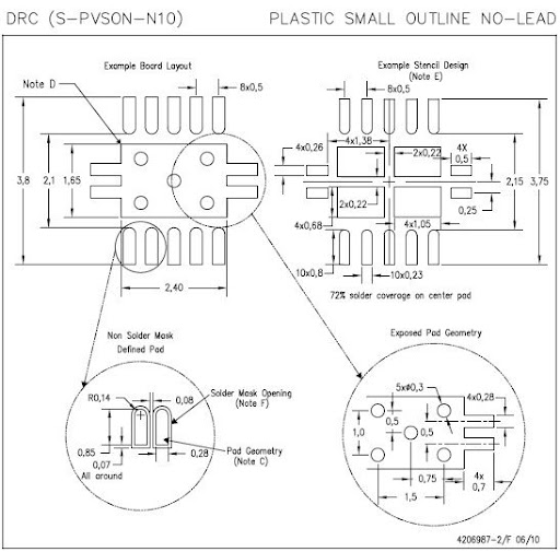
As part of the new design and "new to designing with Cadence" process, I am creating parts for our library and I'm having some trouble with a TI SON part that includes a thermal pad or power pad. Here is a snap shot from the TPS6120:

 TI TPS61202 Footprint

At this point, I've made the pads in the padstack editor (but made them rectangles since I didn't know how to make it a rect at one end and rounded at the other) and used the symbol creation wizard to make a SOIC. To make the thermal pad I placed a filled polygon on the Etch/top layer and it is one large pad with the outline like above.

Question: How do turn my filled polygon into a ground pin (or should I not?) and how do I add the soldermask layer to something I've drawn like this?

Question: How do I add vias to my footprint? My plan was to create the via in the padstack editor then place them in the appropriate places but I have some confusion as to whether the pad/via structure is just supposed to sit there dangling or if it should be assigned a pin # (ground).

I did search the forum and came across the thread Thermal Pad Shape with Vias In it a poster mentions that he makes these pads using multiple surface mount style pins. I think I can figure out how to do this but I'd appreciate any tips on setting up the tools and pads so that things are properly done.

Picture of the pad made from pins:

pad of pins

How to add a company logo or a marking seregraphy with "Allegro PCB Design"

$
0
0

Hi,

how to add a company logo, a picture, or a marking seregraphy in PCB board with "Allegro PCB Design",

see exemple in attached image:


Best regards,


Haithem.


Define BGA Component

$
0
0

In Orcad Capture I want to define the controller STM32L151RB. It has a 5x5mm BGA64 package. When I call "new part" in my library, I have a field, where I can input the PCB Footprint. Can I see an overview of existing footprints ? Can I find the BGA64 anywhere ? Is there any example with this controller ?

Constraints for fanout

$
0
0

Hi, 

I want to create some rules for Allegro PCB when it creates fanout for my BGA. I have defined two types of VIAs and I want to force Allegro to use one VIA - and thick track width -  for Power& GND pads and other VIA - with thinner track width - for signals. Where can I define such rules?

Any suggestions are welcome.

Hossein 

how to use EPC1010 SPICE model in Orcad PSPICE

Capture 16.6: Can't close properties spreadsheet using keyboard under Win7

$
0
0

Hello folks,

I recently was forced to upgrade to Windoze 7 and consequently had to re-install OrCAD PCB Designer 16.6.  My problem is that, in Capture, I can no longer use the keyboard to close the property spreadsheet; the only ways I am able to close the properties spreadsheet are either by clicking on the X at the top right (and, if I am not careful, closing the whole application!) or by right-clicking on the tab and selecting close in the context menu.  I used to be able to use CTRL-F4 to do that but it does not work any more.  CTRL-F4 does work to close a schematic tab in a design though but it does not work with the property spreadsheet.  This is just an annoying nuisance.

 Does anybody know what I can do to restore the keyboard shortcut for closing the property spreadsheet?  I cannot find the solution anywhere.

 Thanks in advance.


Thermal Relief doesn't work for Power palnes

$
0
0

Hi,

I have defined circle as Thermal Relief for all layers of my pads. Below are some questions regarding shape drawing in various layaers:

1- Thermal Relief doesn't work for power planes while it works for signal, Top & Bottom Layers. I see that it only uses a zero length cross to connect pad to polygone or shape in power planes (Figure 1)

Figure1

https://drive.google.com/file/d/0BzS3_lT7y4tEekhtX3hoR1dCcU0/edit?usp=sharing

2- Shape in power planes is connected to pins of other nets!.(Figure 2)

Figure2

https://drive.google.com/file/d/0BzS3_lT7y4tEbG9GNFRsQWRmcFU/edit?usp=sharing

3- After changing constraints shapes or polygones seem to be connected directly to pads!. How can I make sure that all constraints are applied after any shape or constraint edit (Figure 3)

Figure3

https://drive.google.com/file/d/0BzS3_lT7y4tEc2V5VUlfOG5MVFE/edit?usp=sharing

4- Where can I change settings for thermal pads? I mean "connect width" and "gap" between plane and pad (Figure 4)

Figure4

https://drive.google.com/file/d/0BzS3_lT7y4tEUVBjbkFvdWgxdW8/edit?usp=sharing

5- Do I have to use Shape-> Check for all shapes or polygones everytime I make changes in Constraint Manager or there is a much easier way for it?

I am very short of time. So, I need urgent help.

Thanks all in advance,

Hossein

broken help, allegro capture, "can't find tag file"

$
0
0

 I'm attempting to get "Help" working on our Allegro Design Entry CIS 16.5.   Currently the F1 key or the Capture Help menu just brings up an error CAN'T FIND TAG FILE, as well as the usual tabtips.

 Might this be a common problem with a known solution?


Rats with Various colors

$
0
0

Hi,

I don't see why Allegro PCB shows some Rats in red color and some others in default blue color. I see that it shows squre for VCC, GND nets. Presumably, it has happend after setting some constraints in CM. Does anybody know about it? Attached picture shows some nets with various colors.


Thanks in advance,

Hossein


bare die on pcb

$
0
0

Hello,

I have a question similar to the one posed in http://www.cadence.com/Community/forums/t/20786.aspx .

In my design I will have bare silicon chips directly mounted on the pcb (flex pcb) in a rather complex 3d setup. Those chips have wirebond pads which will be naturally connected by wirebonds to the corresponding pads on the flex. What is the best way to proceed? From what I have found, I suppose I have to create a new part in the part designer with a completely self drawn footprint for each chip and to define the wirebond pads together with a wirebond layer in their padstacks? I searched through the documentation but did not find anything resembling exactly this situation. I would be grateful if someone could point me to an appropriate example.

Thank you very much.

Failed to get Creo Export Installation Path

$
0
0

Hello All,

 I'm using  ORCAD PCB editor 16.6 and I couldn't make the "Creo View" work. I installed the "Creo View Interface for ECAD" without any errors but when I try to run the Creo View in the ORCAD, it display "Failed to get Creo Export Installation Path". Any answer is highly appreciated. Thanks

How to change the order of schematic pager

$
0
0

 Hi,

I have a 10 schematic pages in my design. I want to change the order of them (re sequence). For example the 5th page should go to 7th place etc. Help me how to do it.

Gilbert

Cadence tools opening very slowly

$
0
0

 Hi, In my PC Cadence tools, from concept HDL to Allegro PCB designer. atleast it is taking 15 minutes. I disabled Open Gl, I set CDS_LIC_ONLY variable also. What could make cadence too slow. Please Help. I have Windows 8, 6GB RAM. Is it problem with OS. I am using Allegro 16.5


Regards,

Anil Kumar 

Constraints for fanout

$
0
0

Hi, 

I want to create some rules for Allegro PCB when it creates fanout for my BGA. I have defined two types of VIAs and I want to force Allegro to use one VIA - and thick track width -  for Power& GND pads and other VIA - with thinner track width - for signals. Where can I define such rules?

Any suggestions are welcome.

Hossein 

Viewing all 5525 articles
Browse latest View live


<script src="https://jsc.adskeeper.com/r/s/rssing.com.1596347.js" async> </script>